Optical closed-loop control system for a CMP apparatus and method of manufacture thereof

Active Publication Date: 2006-01-31
VERITY INSTR
View PDF30 Cites 62 Cited by
  • Summary
  • Abstract
  • Description
  • Claims
  • Application Information

AI Technical Summary

Problems solved by technology

As with any physical process, however, there are imperfections in the processes that can contribute to non-planarity of the wafer.
Excessive or improper polishing may

Method used


Image

  • Optical closed-loop control system for a CMP apparatus and method of manufacture thereof
  • Optical closed-loop control system for a CMP apparatus and method of manufacture thereof
  • Optical closed-loop control system for a CMP apparatus and method of manufacture thereof

Examples


Embodiment Construction

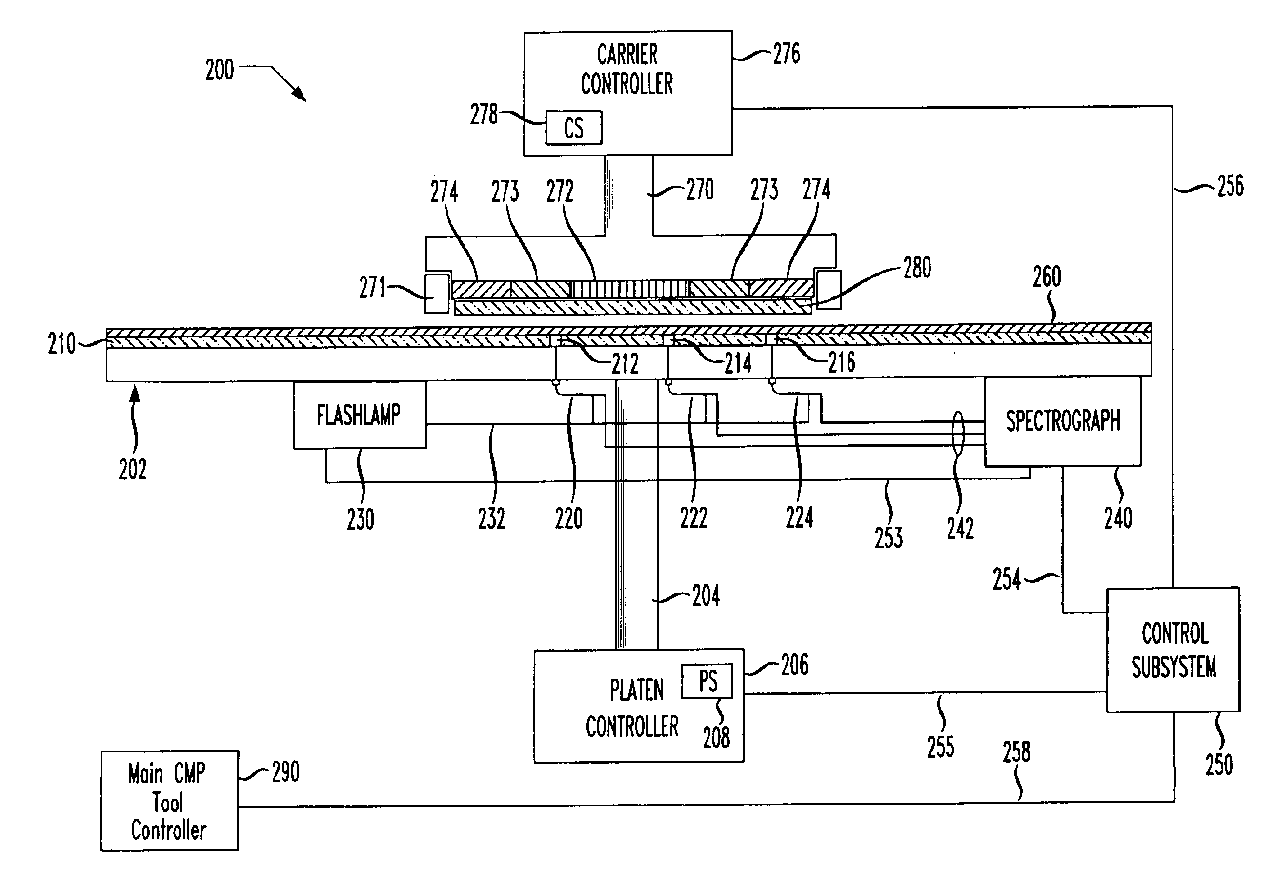
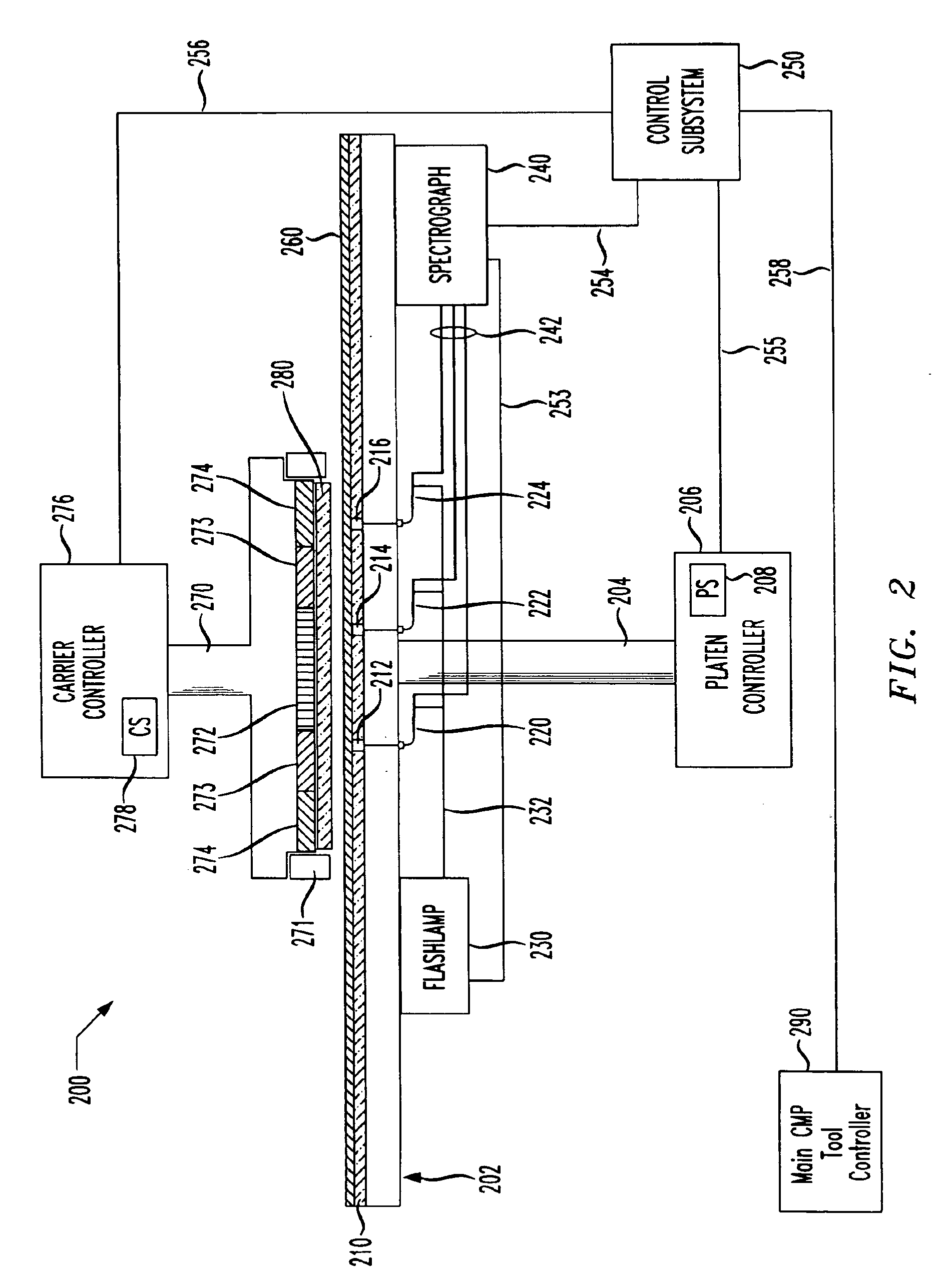
[0042]Referring initially to FIG. 2, illustrated is an optical closed-loop control system, generally designated 200, for use with a chemical mechanical polishing (CMP) apparatus constructed in accordance with the principles of the present invention. Although the current embodiment is illustrated using a conventional rotary-type platen type CMP polisher, the invention may be used with other types of CMP polishers that are well known in the art, such as orbital and fixed platen systems. In one embodiment, the CMP apparatus includes a platen 202 and coupled to a top surface of the platen 202 is a conventional polishing pad 210. The platen 202 is also coupled to a spindle 204. The spindle 204 may be coupled to a platen controller 206 that is configured to cause translations, rotations, orbits or other compound movements of the platen 202 and spindle 204. The platen controller 206 also includes at least one platen sensor 208 that is configured to monitor the location of the platen 202 an...


PUM

PropertyMeasurementUnit
Distanceaaaaaaaaaa
Pressureaaaaaaaaaa
Interferenceaaaaaaaaaa

Abstract

For use with a chemical mechanical polishing apparatus for polishing a semiconductor wafer having a platen, a polishing pad and a wafer carrier, an optical closed-loop control system. In one embodiment, the system includes a plurality of optical probes impacting a corresponding probe window and rigidly mountable through the platen. The system also includes a flash lamp configured to provide light to each of the plurality of optical probes and minimize an exposure time of the light onto the semiconductor wafer, a spectrograph configured to spatially image light received by each of the plurality of optical probes to a common charge-coupled device and produce real-time spectral reflectometry data therefrom. The system further includes a control subsystem configured to analyze the real-time spectral reflectometry data and determine at least one wafer state parameter therefrom, and cause the polishing to be adjusted based upon the at least one wafer state parameter.

Description

TECHNICAL FIELD OF THE INVENTION[0001]The present invention is directed, in general, to a semiconductor wafer polishing apparatus and, more specifically, to an optical closed-loop control system for use with a chemical mechanical polishing apparatus for polishing a semiconductor wafer.BACKGROUND OF THE INVENTION[0002]The manufacture of an integrated circuit device requires the formation of various materials onto a base substrate to form necessary circuit structures. During the manufacturing process, chemical-mechanical polishing (CMP) is employed to remove certain layers or reduce a layer to a precise thickness. More specifically, CMP employs the combination of chemical etching and mechanical abrasion to remove excess material. In the case of dielectric films, CMP is typically employed to planarize the surface. For metal films, such as copper, CMP is typically used to remove excess material so as to permit the delineation of electrically isolated circuit interconnects. Also, it migh...

Claims


Application Information

Patent Timeline
IPC IPC(8): B24B49/00B24B51/00
CPCB24B49/12B24B37/013
Inventor MELONI, MARK A.KUENY, ANDREW W.
Owner VERITY INSTR
Why Eureka
Try Eureka