Shielded probe apparatus for probing semiconductor wafer

a probe apparatus and shielded technology, applied in the field of shielded probe apparatus for probing semiconductor wafers, can solve the problems of difficult to test the characteristics of semiconductor devices in a wide operating temperature range, and achieve the effect of eliminating triboelectric noise and reducing external electrical interferen

a probe apparatus and shielded technology, applied in the field of shielded probe apparatus for probing semiconductor wafers, can solve the problems of difficult to test the characteristics of semiconductor devices in a wide operating temperature range, and achieve the effect of eliminating triboelectric noise and reducing external electrical interferen

US6992495B2Active Publication Date: 2006-01-31CELADON SYST

Image

  • Shielded probe apparatus for probing semiconductor wafer
  • Shielded probe apparatus for probing semiconductor wafer
  • Shielded probe apparatus for probing semiconductor wafer

Examples


Embodiment Construction

[0020]In the following description of a preferred embodiment, reference is made to the accompanying drawings, which form a part hereof, and in which is shown by way of illustration a specific embodiment in which the invention may be practiced. It is to be understood that other embodiments may be utilized and structural changes may be made without departing from the scope of the present invention.

[0021]For purposes of explanation, numerous specific details are set forth in the following description in order to provide a thorough understanding of the present invention. However, it will be evident to one of ordinary skill in the art that the present invention may be practiced without some of these specific details. In other instances, well-known structures and devices are shown in block diagram form in order to facilitate description.

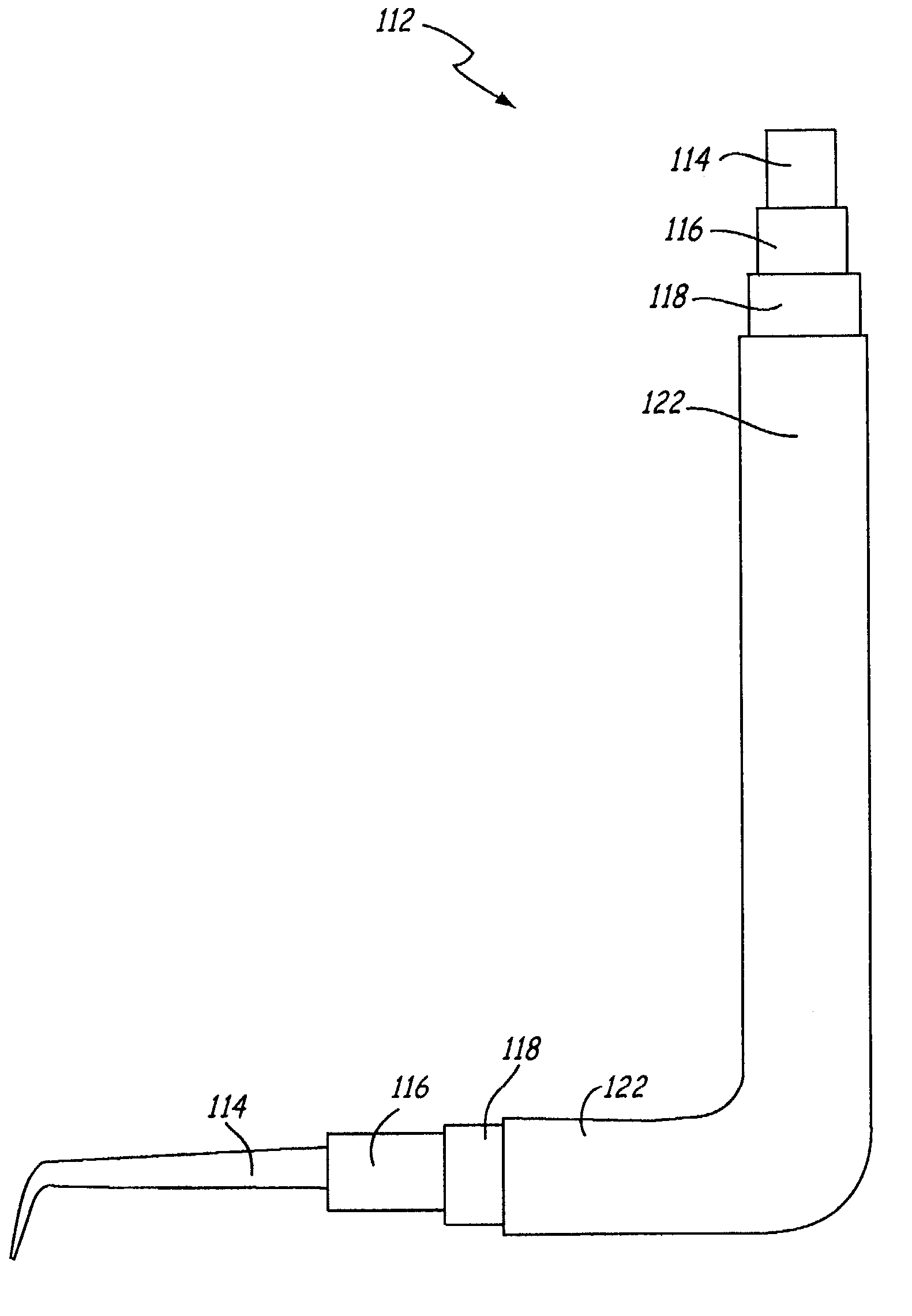
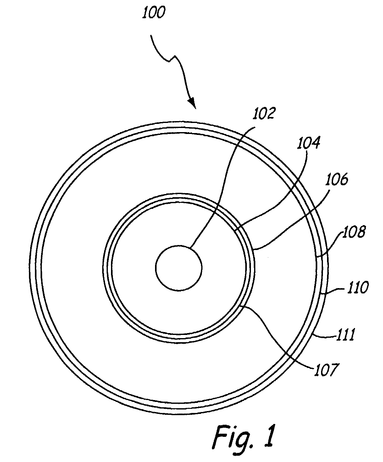
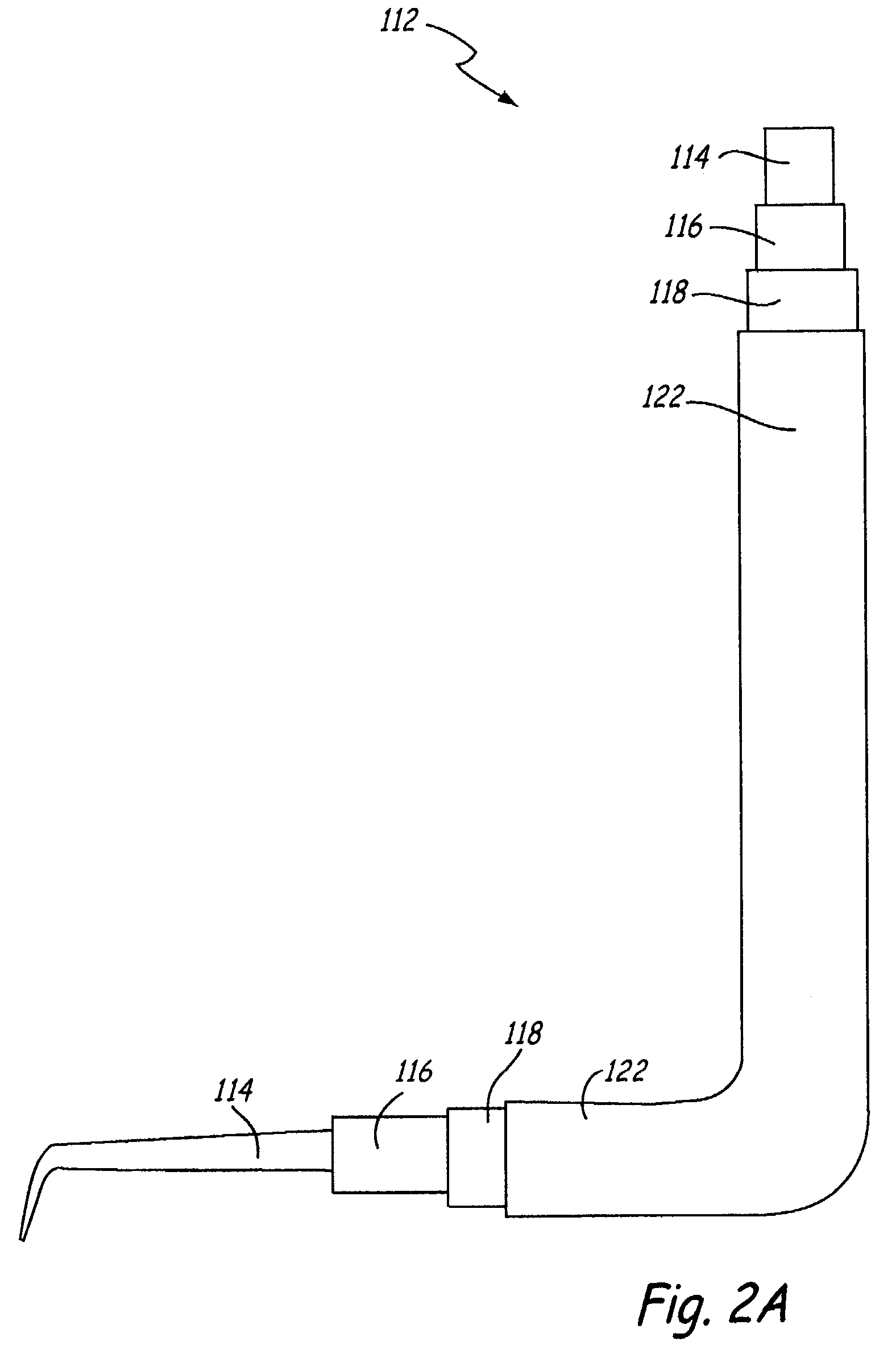
[0022]The present invention utilizes the center signal conductor, guard layer, and ground of a tri-axial cable provided by semiconductor test equipment or...


PUM


Abstract

A shielded probe apparatus is provided with a shielded probe and a tri-axial cable that are electrically connected within a shielded chassis. The shielded probe apparatus is capable of electrically testing a semiconductor device at a sub 100 fA operating current and an operating temperature up to 300 C.

Description

CROSS-REFERENCE TO RELATED APPLICATION(S)[0001]This is a utility patent application which claims priority of U.S. provisional patent application Ser. No. 60 / 392,394, filed Jun. 28, 2002; subject matter of which is incorporated herewith by reference.FIELD OF THE INVENTION[0002]The present invention relates generally to semiconductor test equipment, and more particularly, to a shielded probe used in semiconductor test equipment for electrically probing devices on a semiconductor wafer.BACKGROUND OF THE INVENTION[0003]The semiconductor industry has a need to access many electronic devices on a semiconductor wafer. As the semiconductor industry grows and devices become more complex, many electrical devices, most commonly semiconductor devices, must be electrically tested, for example, for leakage currents and extremely low operating currents. These currents are often below 100 fA. In addition, the currents and device characteristics are often required to be evaluated over a wide tempera...

Claims


Application Information

Patent Timeline
31 Jan 2006
Publication
US6992495B2
IPC
G01R31/02; G01R31/00; G01R1/067; G01R1/18
CPC
G01R1/067; G01R1/18; G01R1/06711
Inventors
ROOT, BRYAN J.; FUNK, WILLIAM A.