
RF module and method for arranging through holes in RF module

a technology of rf module and rf module, which is applied in the direction of resonators, semiconductor devices, semiconductor/solid-state device details, etc., can solve the problems of conductor loss, radiation loss, and the like, and the relationship between the interval of providing through holes and conductor loss has not been accurately clarified from mathematical

Active Publication Date: 2006-01-31
TDK CORPARATION
View PDF16 Cites 12 Cited by
  • Summary
  • Abstract
  • Description
  • Claims
  • Application Information

AI Technical Summary

Benefits of technology

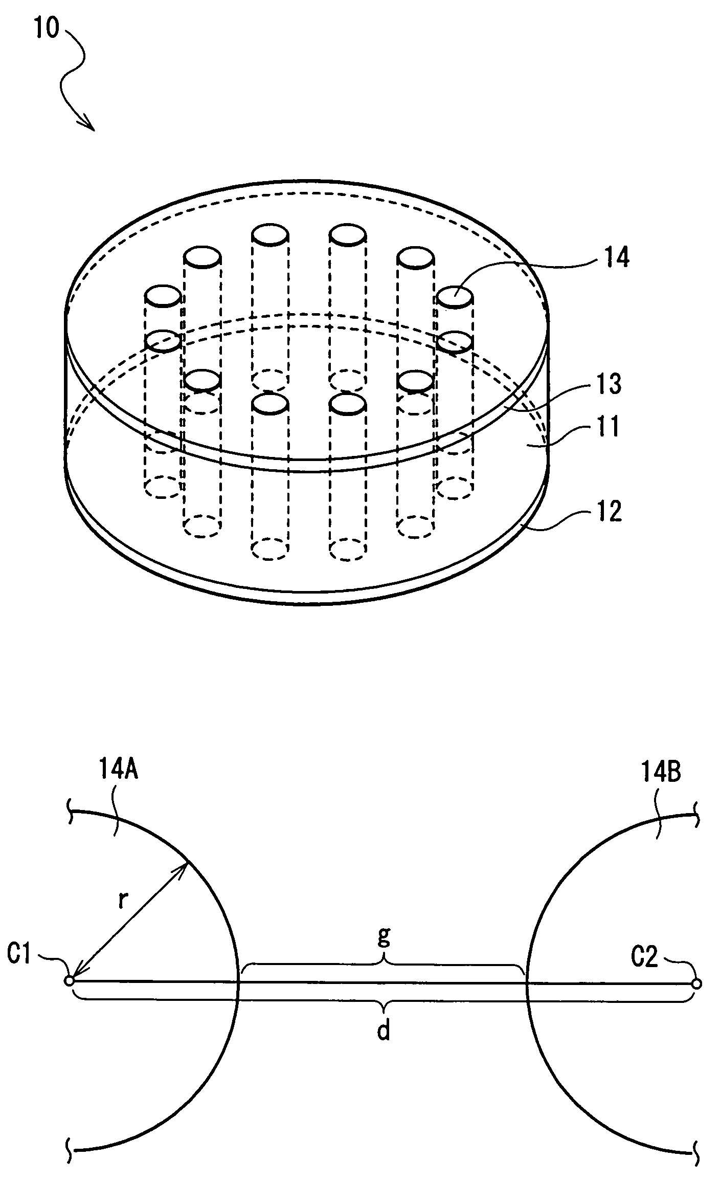
The present invention provides an RF module and a method of arranging through holes in the RF module that optimize the propagation of electromagnetic waves. The through holes are arranged based on a conditional expression that specifies the relation between the interval between centers of neighboring through holes and the radius of each through hole. This arrangement optimizes the relation between the through holes and the signal wavelength, and it also takes into account the non-propagation region between neighboring through holes. The RF module and the method of arranging through holes in the RF module according to the invention provide efficient and effective communication for electromagnetic waves.

Problems solved by technology

However, particularly, the relation between the intervals of providing through holes and a conductor loss, a radiation loss, and the like has not been accurately clarified from mathematic viewpoint.

Method used


Image

  • RF module and method for arranging through holes in RF module
  • RF module and method for arranging through holes in RF module
  • RF module and method for arranging through holes in RF module

Examples


Embodiment Construction

[0042]Embodiments of the invention will now be described in detail hereinbelow with reference to the drawings.

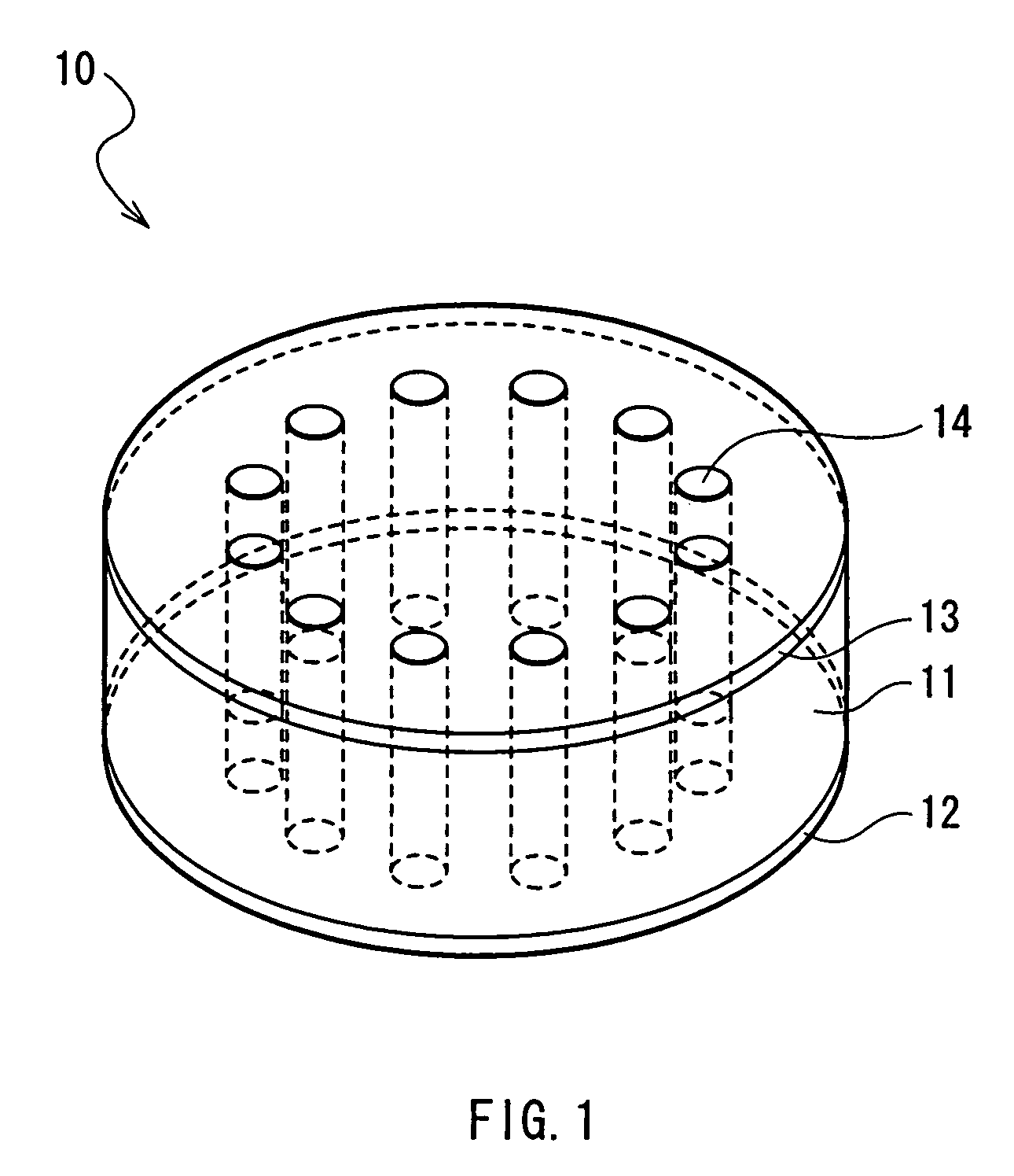
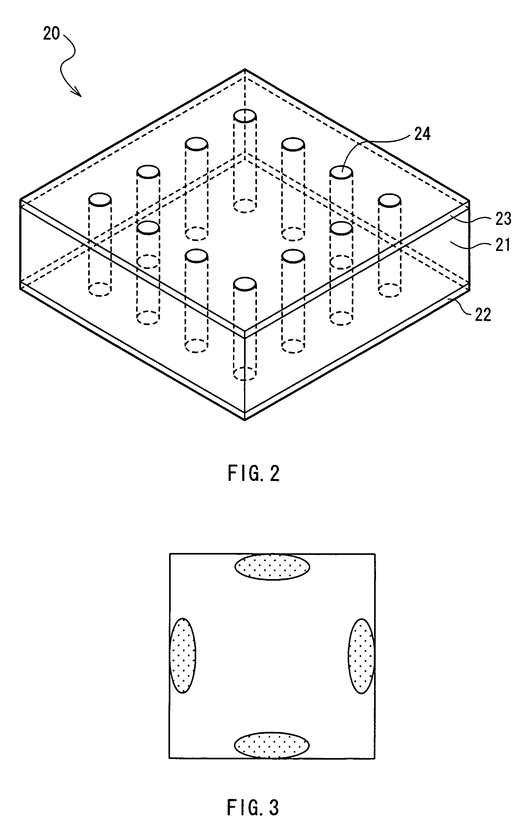
[0043]FIGS. 1 and 2 are diagrams for explaining the configuration of an RF module according to an embodiment of the invention and show simplified main components of the RF module. In both of examples of configuration of FIGS. 1 and 2, the RF modules have a layer-stacked-type waveguide structure using through holes. In FIG. 1, an electromagnetic wave propagation region has a cylindrical shape as a whole. In FIG. 2, an electromagnetic wave propagation region has a rectangular parallelepiped shape as a whole. An RF module using any of the layer-stacked-type waveguide is combined with another transmission line, a resonator, and the like and is used as, for example, a transmission line, a filter, or the like for a high frequency signal.

[0044]A cylindrical waveguide 10 has a dielectric substrate 11, ground electrodes 12 and 13 which face each other while sandwiching the dielectric...


PUM


Abstract

The present invention is directed to optimize arrangement of through holes and enable electromagnetic waves to be efficiently propagated. A cylindrical waveguide has a dielectric substrate, ground electrodes which face each other, and a plurality of through holes for bringing the ground electrodes into conduction. In the case of determining arrangement of the through holes, first, the relation between a center interval and the radius of each of the through holes is obtained from required attenuance of electromagnetic waves. On the basis of the obtained relation, arrangement of the through holes is determined. Irrespective of a signal wavelength and the like conventionally used as parameters, the arrangement of the through holes can be optimized.

Description

BACKGROUND OF THE INVENTION[0001]1. Field of the Invention[0002]The present invention relates to an RF module used for propagating a signal in a high frequency band of microwaves, millimeter waves, or the like and a method for arranging through holes in an RF module.[0003]2. Description of the Related Art[0004]Conventionally, as transmission lines for transmitting a high frequency signal in a microwave band, a millimeter wave band, and the like, a strip line, a waveguide, a dielectric waveguide, and the like are known. They are also known as components of a resonator and a filter for high frequency. An example of a module formed by using any of the components for high frequency is an MMIC (Monolithic Microwave Integrated Circuit).[0005]Recently, there is a known structure that a dielectric waveguide line is formed by a layer stacking technique in a circuit board of a multilayer structure. The structure has a plurality of ground conductors stacked while sandwiching dielectrics and th...

Claims


Application Information

Patent Timeline
Patent Type & Authority Patents(United States)
IPC IPC(8): H01P1/207H01P7/06H01L23/12H01P3/12H01P3/127H01P3/16
CPCH01P3/127H01P3/121
Inventor FUKUNAGA, TATSUYA
Owner TDK CORPARATION
Learn More