Signal transmission film, control signal part and liquid crystal display including the film

a technology of signal transmission and control signal, which is applied in the direction of identification means, instruments, optics, etc., can solve the problems of inferior devices and damage to high-voltage signal wires

Inactive Publication Date: 2006-01-31
SAMSUNG DISPLAY CO LTD
View PDF10 Cites 8 Cited by
  • Summary
  • Abstract
  • Description
  • Claims
  • Application Information

AI Technical Summary

Benefits of technology

[0012]It is an object of the present invention to provide a signal transmission film, a control signal part and a

Problems solved by technology

However, this potential difference causes an electrolysis reaction with moistures permeated into the wires during manufacturing and operatin

Method used


Image

  • Signal transmission film, control signal part and liquid crystal display including the film
  • Signal transmission film, control signal part and liquid crystal display including the film
  • Signal transmission film, control signal part and liquid crystal display including the film

Examples


first embodiment

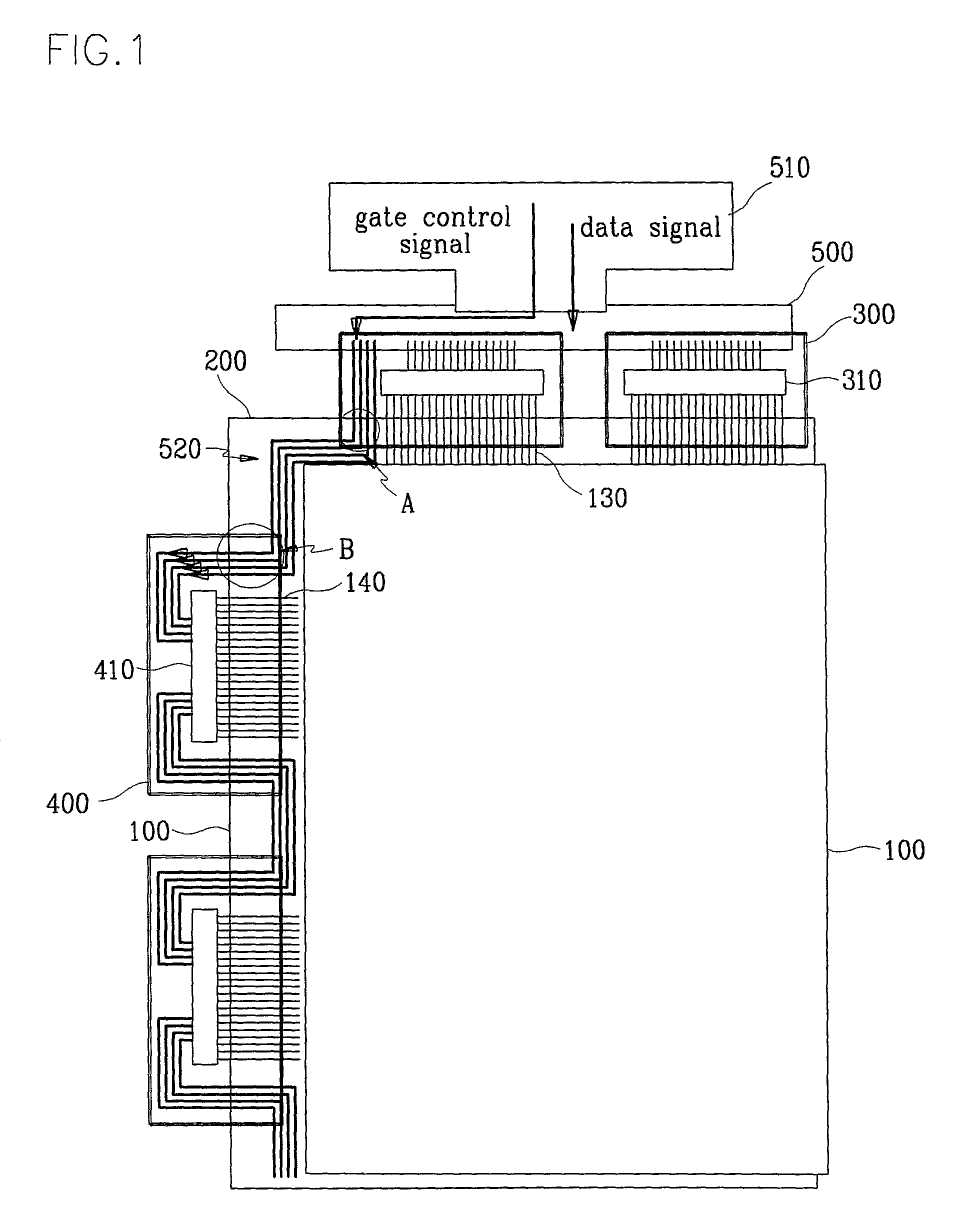
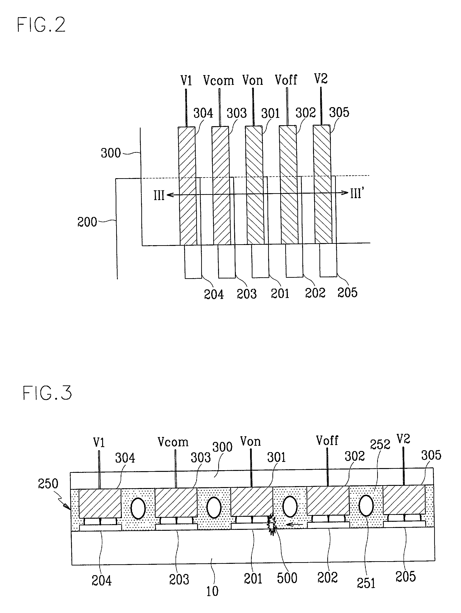
[0080]FIG. 4 is a plan view of a control signal part according to the present invention and FIG. 5 is a cross-sectional view of the control signal part along the line V–V′ of FIG. 4.

[0081]A data signal transmission film 300 with gate control signal leads 301, 302, 303 and high voltage redundancy leads 310 and 320 is attached to a thin film transistor substrate 200 with gate control signal wires 201, 202, 203 using an anisotropic conducting film 250 consisting of conductive materials 251 and an adhesive resin 252. Herein, the wires 201, 202, and 203 of the thin film transistor substrate 200 are electrically connected to the leads 301, 302 and 303 of the data signal transmission film 300 in a one to one correspondence through conductive materials 251 of the anisotropic conducting film 250.

[0082]In the data signal transmission film 300, a high voltage signal lead 301 transmitting a gate-on-voltage, a low voltage signal lead 302 transmitting a gate-off-voltage, a common voltage signal l...

third embodiment

[0100]FIG. 8 is a plan view of an liquid crystal display according to the present invention and FIG. 9 is a cross-sectional view of the liquid crystal display along the line IX–IX′ of FIG. 8.

[0101]In the liquid crystal display of the third embodiment of the present invention, control signal wires transmitting a gate control signal are formed by conductive materials for forming data wire and high voltage dummy wires corresponding to the high voltage dummy leads are not formed.

[0102]A gate wire 20, 21 and 22 comprising a gate line 20 including a gate electrode 22 and a gate pad 21 connected to the end of the gate line 20 is formed on an insulating substrate 10.

[0103]The gate line 20 extends in a horizontal direction and transmits the gate signal outputted from a gate driving integrated circuit (not shown) to pixel region. The gate wire 20, 21 and 22 could be formed by conventional conductive materials such as one of copper family, one of silver family, one of chromium family, or one o...

fourth embodiment

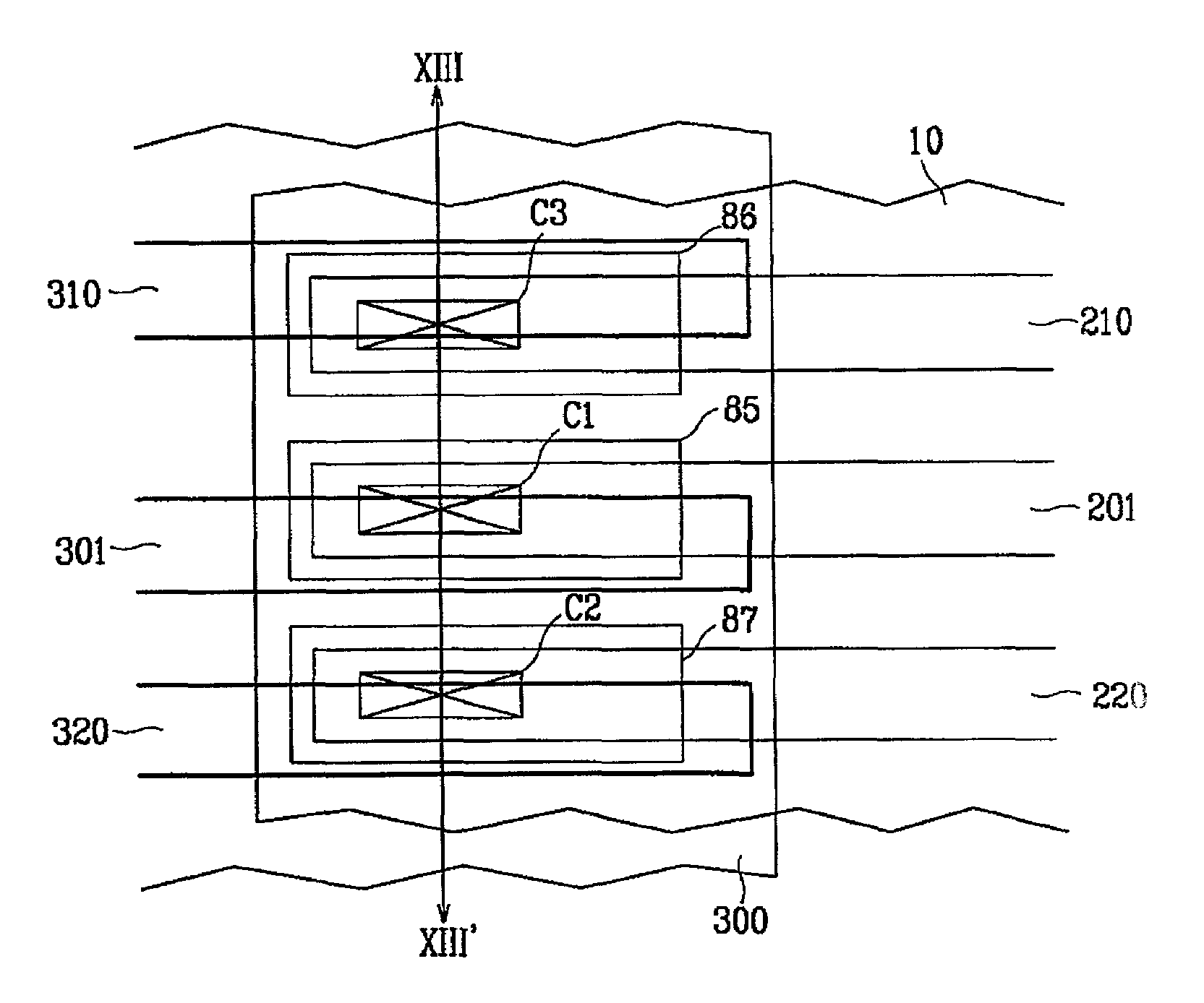
[0135]In the liquid crystal display according to the present invention, the gate control signal wires 201, 202 and 203 are formed by conductive materials for forming the data wire 60, 61, 62 and 63 and the high voltage dummy wires 210 and 220 are formed by conductive materials for forming the pixel electrode such as ITO or IZO.

[0136]FIG. 10 is a plan view of the selected one gate control signal wire of the gate control signal wires and FIG. 11 is a cross sectional view along the line XI–XI′ of FIG. 10.

[0137]When the fourth embodiment is compared with the third embodiment of the present invention, a structure of the display region is identical but a structure of the gate control signal part is different. Accordingly, the structure of the gate control signal part will be described except for the structure of the display region.

[0138]A gate insulating layer 30 is formed on an insulating layer 10 and gate control signal wires 201, 202 and 203 consisting of conductive materials for formi...


PUM


Abstract

The present invention provides a signal transmission film, a control signal part and a liquid crystal display including the signal transmission film that prevents the damage of wires due to electrolysis. In the present invention, a lead of several to several tens microns are formed on the signal transmission film by printing and patterning a copper wire on a high molecular film. The signal transmission film comprises a first signal lead transmitting a first signal voltage; a second signal lead transmitting a second signal voltage lower than the first signal voltage; and a lead formed between the first signal lead and the second signal lead. The lead could be several to several tens microns thick, the same voltage as the first signal voltage could be applied to the lead and the lead could be a dummy lead.

Description

BACKGROUND OF THE INVENTION[0001](a) Field of the Invention[0002]The present invention relates to signal transmission film, a control signal part and a liquid crystal display including the signal transmission film.[0003](b) Description of the Related Art[0004]A liquid crystal display is one of the flat display devices widely used at the present time. The liquid crystal display comprises two substrates on which a plurality of electrodes are formed, a liquid crystal layer sandwiched between the two substrates and two polarizing films for polarizing the light attached to each outward surface of the substrates. The liquid crystal display controls the light transmittance, thereby to display picture images by applying different voltages to the electrodes while forming electric fields for varying the orientation of the liquid crystal molecules of the liquid crystal layer. In such a liquid crystal display, thin film transistors are formed in one of the two substrates, which is called as a T...

Claims


Application Information

Patent Timeline
IPC IPC(8): G02F1/1345G02F1/13G02F1/1362G09F9/00G09F9/30G09F9/35
CPCG02F1/1345G02F1/1362G02F1/13458G02F1/13
Inventor KIM, DONG-GYUKANG, SIN-KU
Owner SAMSUNG DISPLAY CO LTD
Why Eureka
Try Eureka