

Measuring an alignment target with a single polarization state
a single polarization state and alignment target technology, applied in the field of alignment metrology, can solve the problems of reducing alignment tolerances, becoming increasingly difficult to measure the alignment accuracy of one masking level to the previous level, and increasing the difficulty of overlay metrology problems
- Summary
- Abstract
- Description
- Claims
- Application Information
AI Technical Summary
Problems solved by technology
Method used
Image

Examples
Embodiment Construction
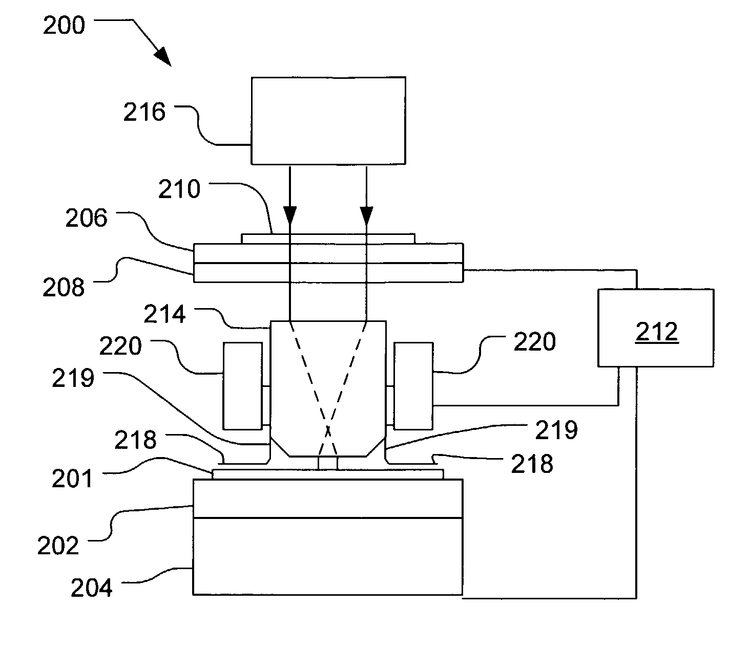
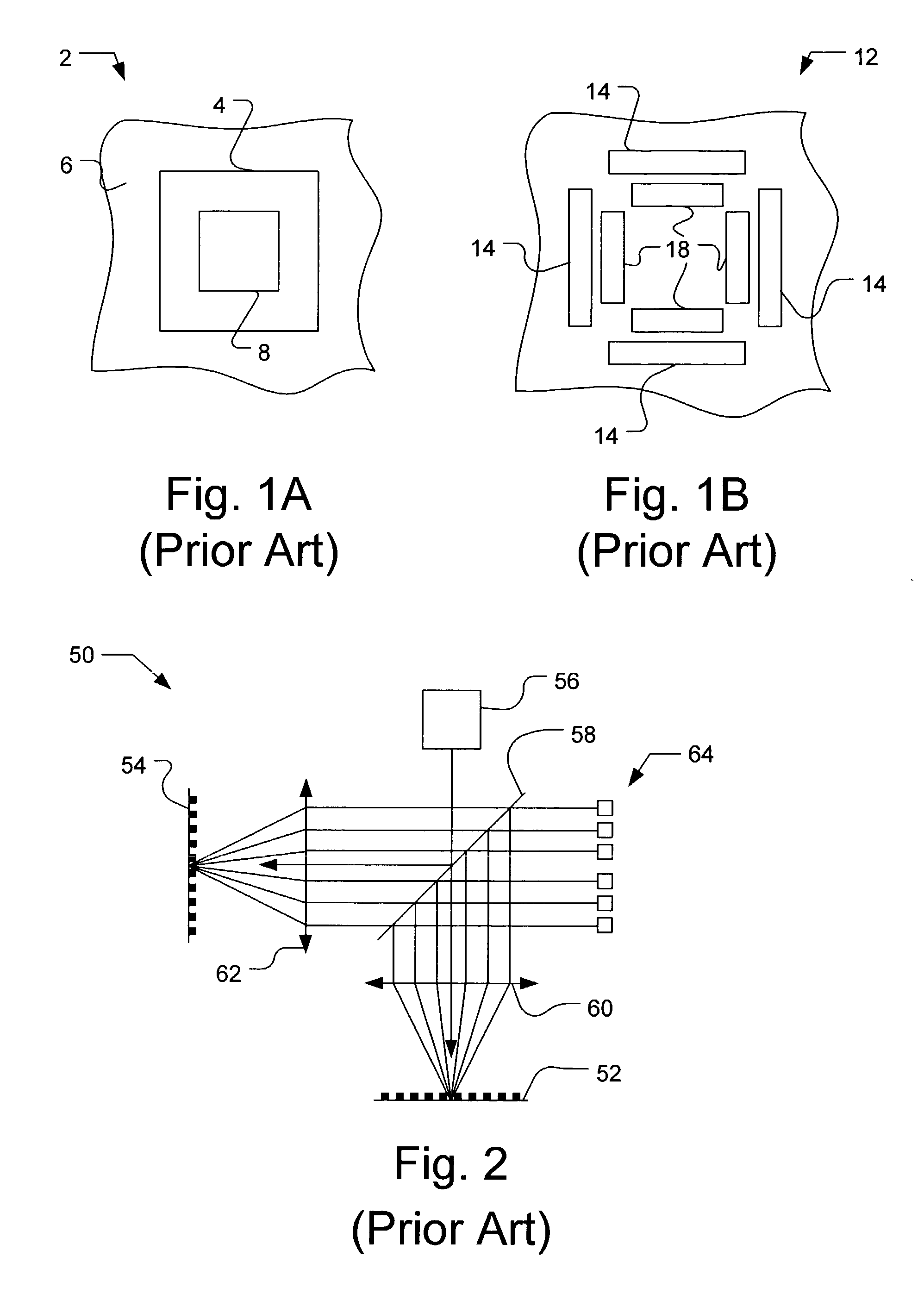
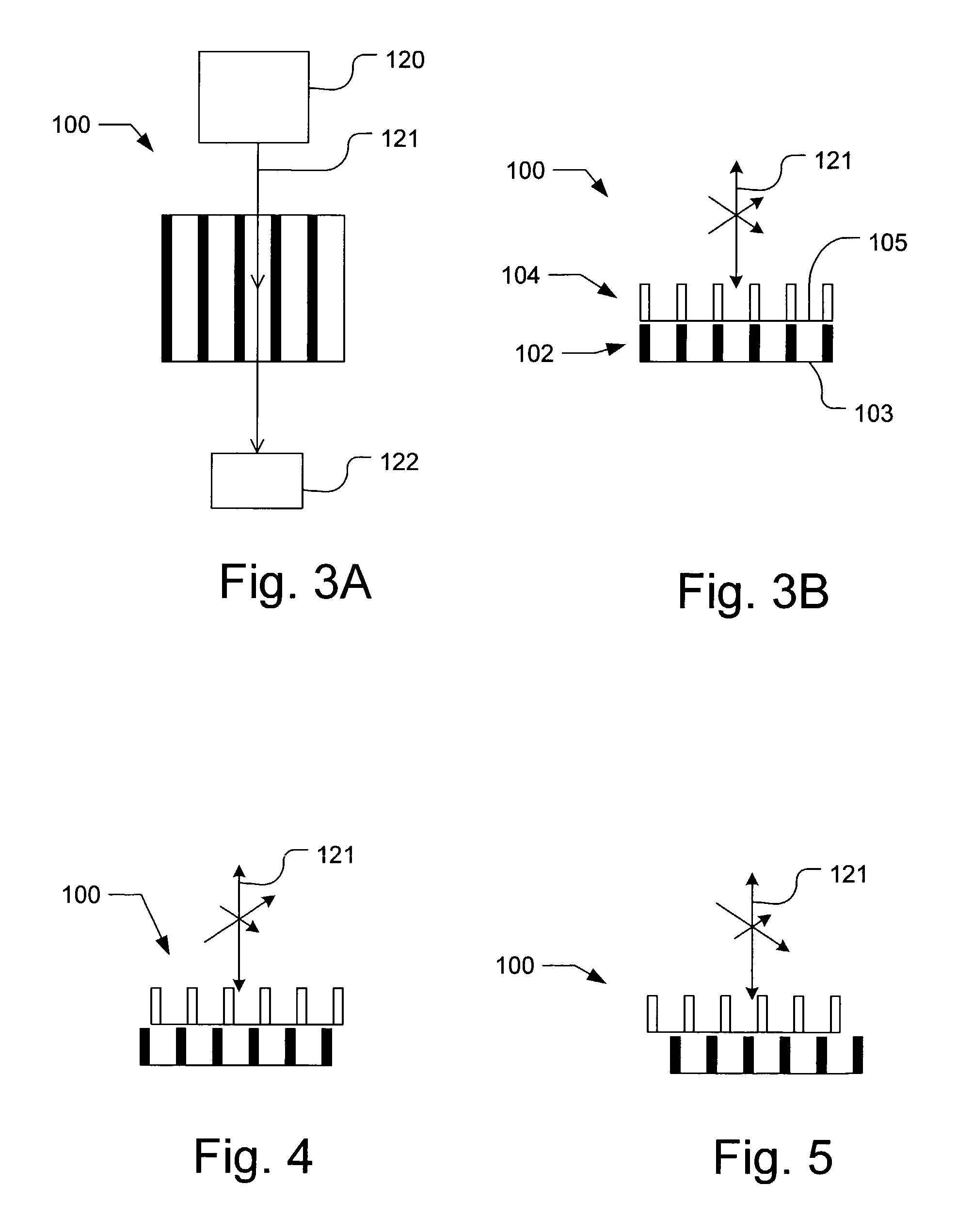
[0035]An alignment target is measured using a single polarization state, in accordance with the present invention, to align two elements. For example, the alignment target can be used to align a substrate and / or a reticle with respect to a stationary element, e.g., the lens, in an exposure tool. Of course, the alignment target is not limited to use in an exposure tool, but may be used to align any two elements. Additionally, the alignment target can be used to measure the amount of alignment error between any two elements, such as two layers on a substrate or any other elements. An alignment target suitable for use with the present invention is described in U.S. patent application “Measuring An Alignment Target with Multiple Polarization States” by Weidong Yang and Roger R. Lowe-Webb, Ser. No. 10 / 116,798, filed Apr. 4, 2002, and which has the same assignee as the present application and is incorporated herein by reference.
[0036]The alignment target and method of use of the present i...
PUM
| Property | Measurement | Unit |
|---|---|---|
| feature sizes | aaaaa | aaaaa |
| distance | aaaaa | aaaaa |
| distance | aaaaa | aaaaa |
Abstract
Description
Claims
Application Information