

Magnetic memory and method for optimizing write current in a magnetic memory
a magnetic memory and write current technology, applied in the direction of digital storage, semiconductor devices, instruments, etc., can solve the problems of large current required for generating the magnetic field, 40 mw of the same mram for writing, and far more power than in the read operation
- Summary
- Abstract
- Description
- Claims
- Application Information
AI Technical Summary
Benefits of technology
Problems solved by technology
Method used
Image

Examples
Embodiment Construction
[0001]1. Field of the Invention
[0002]The present invention relates to methods for optimizing a write current in a magnetic memory device and to a magnetic memory device. More particularly, the present invention relates to methods for optimizing a write current in a magnetic random access memory (hereinafter referred to as MRAM) and to a magnetic memory device.
[0003]2. Background Art
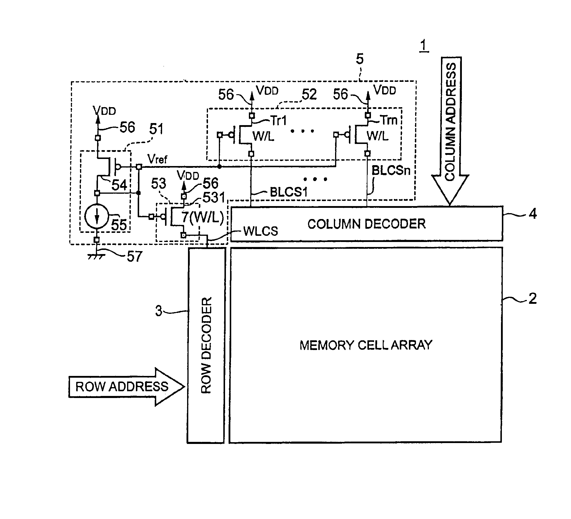
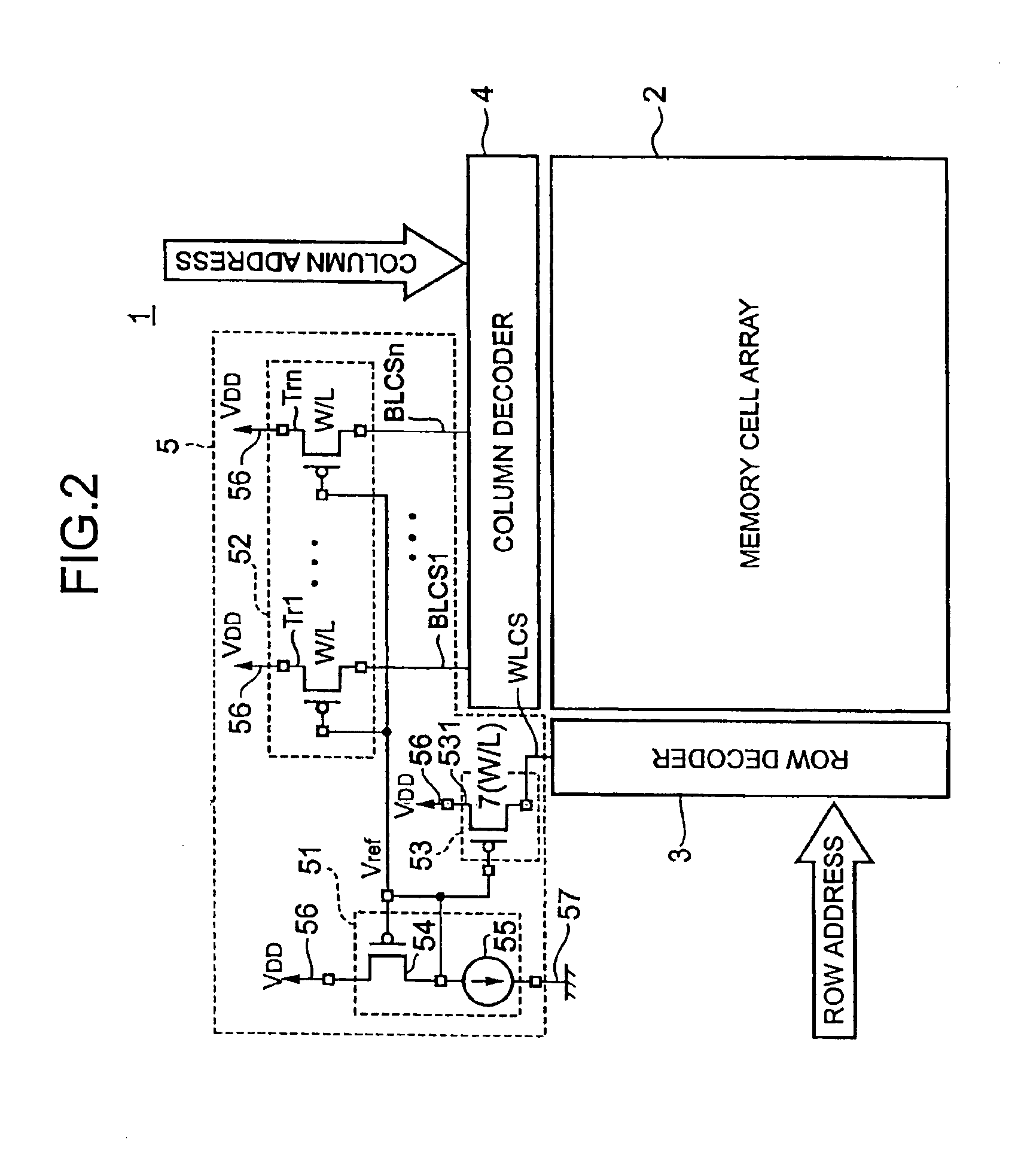
[0004]Currently, an MRAM is receiving attention as a nonvolatile storage. The MRAM uses magnetic tunneling junction (hereinafter referred to as “MTJ”) device as its magnetic memory element.
[0005]FIG. 3 is a sectional view illustrating an exemplary structure of an MRAM memory cell. The memory cell shown in FIG. 3 has an MTJ device 12 and a transistor 50. The transistor 50 is formed on the main surface of a p-type semiconductor substrate 100 typically formed of silicon. On the main surface of the semiconductor substrate 100, n-type diffusion regions 101 and 102 are formed with a predetermined gap provided t...
PUM
 Abstract
Description
Claims
Application Information