Nonvolatile semiconductor memory device and control method thereof

a memory device and nonvolatile technology, applied in semiconductor devices, digital storage, instruments, etc., can solve the problems of power consumption of memory devices, power consumption in standby state, and insufficient battery life of mobile devices such as accessing information, etc., to suppress the increase of current consumption

Active Publication Date: 2006-02-07
SAMSUNG ELECTRONICS CO LTD
View PDF4 Cites 85 Cited by
  • Summary
  • Abstract
  • Description
  • Claims
  • Application Information

AI Technical Summary

Benefits of technology

[0011]The present invention has been made in consideration of the problems and its object is to provide a nonvolatile semiconductor memory device and a control method thereof which can realize reliable programming and erasing of data to / from a memory cell while suppressing increase in current consumption at the time of programming or erasing and in which a memory cell includes a variable resistive element for storing information according to a change in electric resistance caused by application of a voltage.

Problems solved by technology

However, performances of the mobile apparatus such as the life of a battery of the mobile apparatus and access speed to information are not sufficiently high yet and there are unlimited demands for improvements in the performances.
In a mobile apparatus, in an active operation state, power consumption of a logic circuit for executing a logic function is dominant but, in a standby state, power consumption of a memory device is dominant.
The power consumption in the standby state is becoming more important as the drive time by a battery of a mobile apparatus increases.
Those nonvolatile semiconductor memories have tradeoffs among high speed, rewrite resistance, power consumption and the like.

Method used


Image

  • Nonvolatile semiconductor memory device and control method thereof
  • Nonvolatile semiconductor memory device and control method thereof
  • Nonvolatile semiconductor memory device and control method thereof

Examples


first embodiment

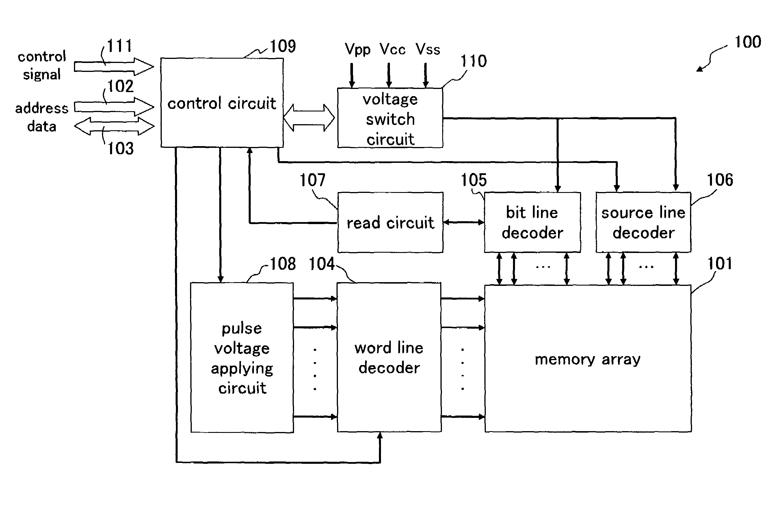
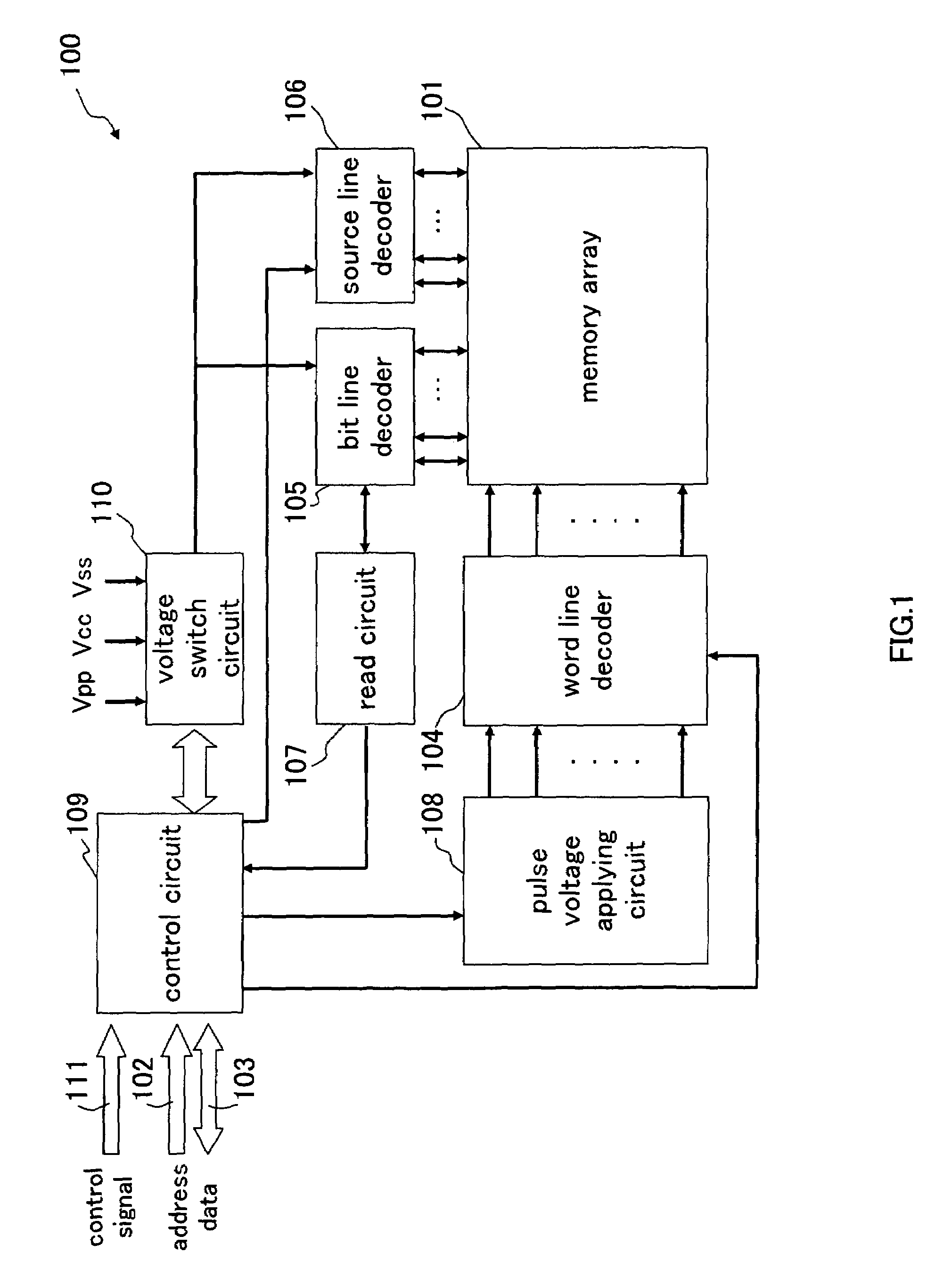
[0041]FIG. 1 is a block diagram of an inventive device 100. The inventive device 100 has a configuration in that information is stored in a memory array 101 and the memory array 101 is constructed by arranging a plurality of memory cells. Information can be stored / read to / from a memory cell in the memory array 101.

[0042]Information is stored into a specific memory cell in the memory array 101 corresponding to an address input from an address line 102. The information passes through a data line 103 and is output to the outside of the device. A word line decoder 104 selects a word line in the memory array 101 corresponding to a signal input to the address line 102, a bit line decoder 105 selects a bit line in the memory array 101 corresponding to an address signal input to the address line 102 and, further, a source line decoder 106 selects a source line of the memory array 101 corresponding to the address signal input to the address line 102. A control circuit 109 controls programmin...

second embodiment

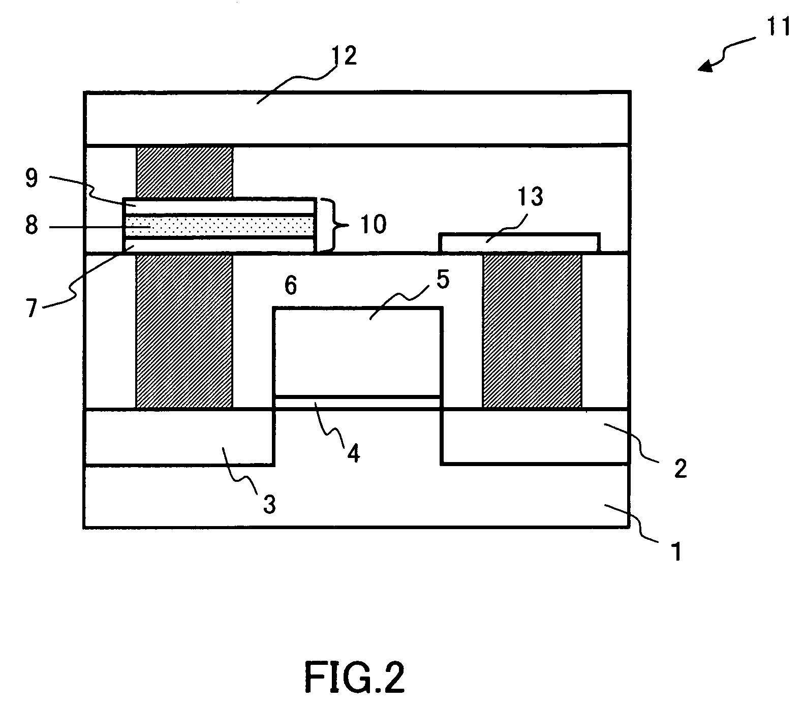
[0084]It has been described above that, in the inventive device and the inventive method according to the first embodiment, at the time of programming and erasing, by independently adjusting the voltage amplitudes Vwp and Vwe of the pulse voltage applied to the gate electrode 5 in the selection transistor 6 in the memory cell 11, the programming and erasing operations can be performed. In the first embodiment, according to the pulse width of the pulse voltage applied to the gate voltage 5, a period in which the memory cell is in the program or erase state is specified. In the inventive device and the inventive method according to a second embodiment, by applying the pulse voltage to one of a bit line and a source line connected to a memory cell to be programmed or erased, the program voltage or erase voltage in pulses to be applied across a bit line and a source line in the first embodiment is applied. During the period, a predetermined word line voltage is applied to a word line co...


PUM


Abstract

A nonvolatile semiconductor memory device includes a memory array in which a plurality of memory cells are arranged in a row direction and a column direction, each of the memory cells being formed by connecting one end of a variable resistive element for storing information according to a change in electric resistance caused by an electric stress and a drain of a selection transistor to each other on a semiconductor substrate, a voltage switch circuit for switching among a program voltage, an erase voltage and a read voltage to be applied to the source line and the bit line connected to the memory cell, and a pulse voltage applying circuit. In the state where the program voltage or erase voltage corresponding to the bit line and the source line is applied to the bit line and the source line connected to a memory cell to be programmed or erased in the memory array via the voltage switch circuit, the pulse voltage applying circuit applies a voltage pulse for programming or erasing to the word line connected to the gate electrode of the selection transistor connected to the memory cell.

Description

BACKGROUND OF THE INVENTION[0001]1. Field of the Invention[0002]The present invention relates to a nonvolatile semiconductor memory device having a memory array in which a plurality of memory cells each formed by connecting one end of a variable resistive element for storing information according to a change in electric resistance caused by application of a voltage and a drain of a selection transistor to each other on a semiconductor substrate are arranged in the row direction and the column direction, and a control method thereof. More particularly, the present invention relates to a method of applying a voltage to a memory cell at the time of programming or erasing.[0003]2. Description of the Related Art[0004]In recent years, it is getting easier and easier to obtain information anytime and anywhere and to freely carry the information. Because of spread of mobile apparatuses typified by a portable telephone and a PDA (Personal Digital Assistant), the user can access various infor...

Claims


Application Information

Patent Timeline
Patent Type & Authority Patents(United States)
IPC IPC(8): G11C11/24G11C7/00G11C16/14G11C11/56G11C13/00G11C16/02G11C16/10G11C16/12H01L27/10H01L45/00
CPCG11C11/5685G11C13/0007G11C13/0064G11C13/0069G11C2213/79G11C2013/0071G11C2013/009G11C2213/31G11C5/063
Inventor MORIMOTO, HIDENORI
Owner SAMSUNG ELECTRONICS CO LTD
Why Eureka
Try Eureka