Method for manufacturing a circuit board

a manufacturing method and circuit board technology, applied in the field of circuit boards, can solve the problems of increasing cost, inability to design circuit boards, and product inability to operate properly, and achieve the effect of less variation

Inactive Publication Date: 2006-02-14
PANASONIC CORP
View PDF10 Cites 14 Cited by
  • Summary
  • Abstract
  • Description
  • Claims
  • Application Information

AI Technical Summary

Benefits of technology

[0016]It is an object of the present invention to solve the problems described above and to provide a circuit board and a method for manufacturing the same that can achieve a high-density wiring and an inner via connection resistance with less variation even when a base material including a reinforcer sheet with density distribution in its in-plane direction such as a glass-epoxy base material is used for an insulator layer.
[0019]According to the present invention, it becomes possible to provide a circuit board and a method for manufacturing the same that can achieve a high-density wiring and an inner via connection resistance with less variation even when a base material including a reinforcer sheet with density distribution in its in-plane direction such as a glass-epoxy base material is used for an insulator layer.

Problems solved by technology

Accordingly, if the circuit resistance varies from one product to another, this causes a problem in that the circuit design is impossible or that the circuit resistance of the product deviates from a designed value so that the product cannot operate properly.
However, the above-described circuit board technology having the inner-via-hole structure over all the layers has had a following problem.
Such management would increase cost.
However, when simply attempting to apply the above-described inner-via-hole technology over all the layers to the glass-epoxy base material, there arises a problem in that the variations in the connection resistance of the inner via holes increase.
Consequently, a sufficient compression force is not applied in the longitudinal direction of the inner via hole, so that electrical conductors cannot be connected sufficiently, thus increasing an electrical connection resistance.

Method used


Image

  • Method for manufacturing a circuit board
  • Method for manufacturing a circuit board
  • Method for manufacturing a circuit board

Examples


first embodiment

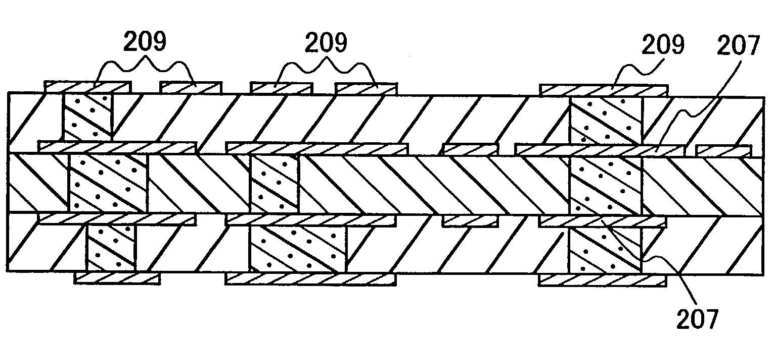
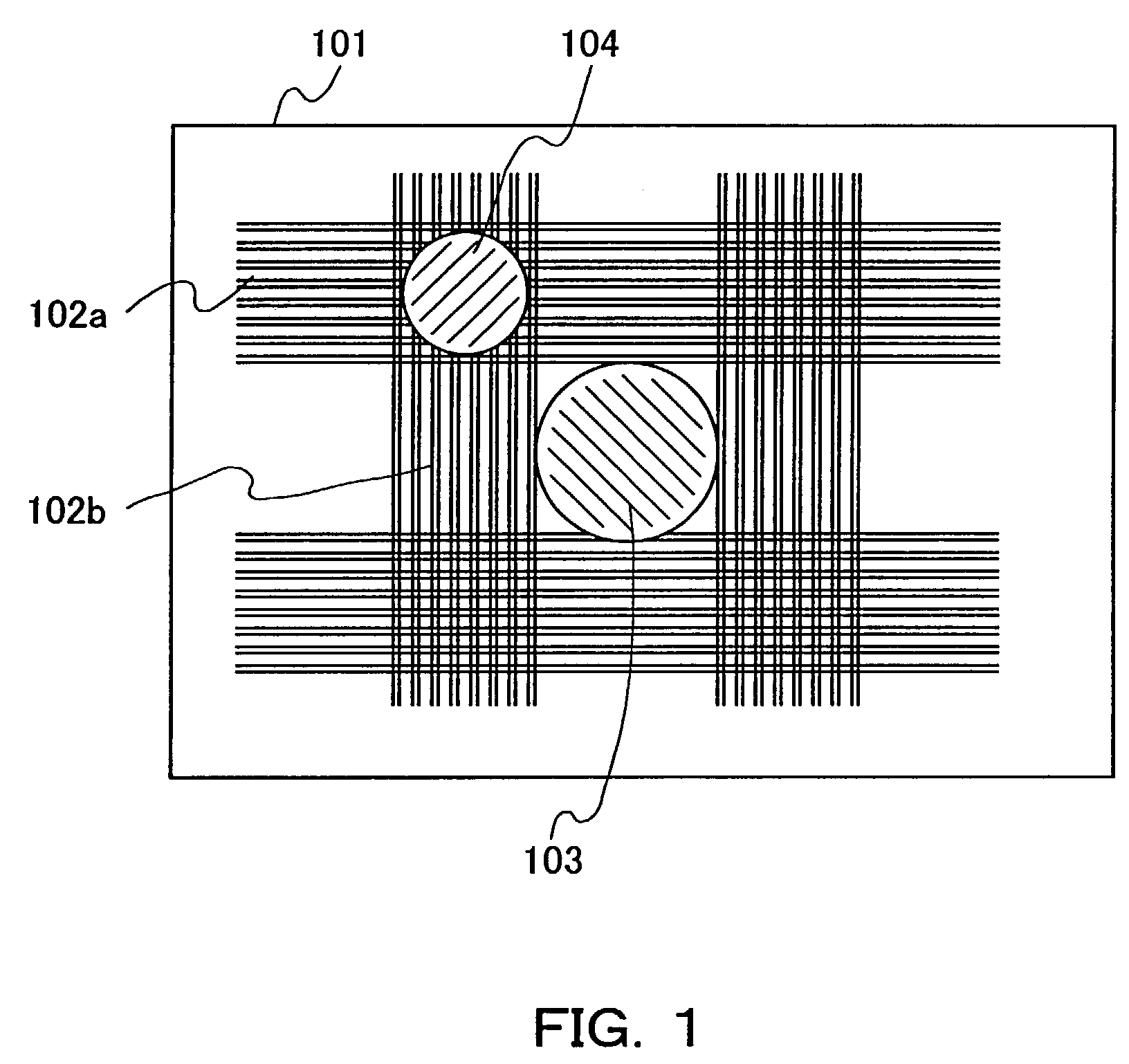
[0072]FIG. 1 is a schematic plan view showing a circuit board of the first embodiment. The present embodiment is directed to the case in which a glass-epoxy base material is used for an insulator layer including a reinforcer sheet 101 with density distribution in its in-plane direction. To facilitate an explanation, FIG. 1 shows wefts 102a and warps 102b of a glass woven fabric inside the base material. An inner via hole 103 that is provided in a portion other than an overlapping portion of glass fibers (a high-density portion of the reinforcer sheet) has a larger cross-section than an inner via hole 104 provided in the overlapping portion. In this embodiment, the cross-section of the inner via hole 103 in the sparse portion of the glass cloth is preferably at least 1.15 times, more preferably at least 1.4 times as large as that of the inner via hole 104 in the overlapping portion thereof. Within this range, the variation in via resistance is reduced.

[0073]A circuit board of the pre...

second embodiment

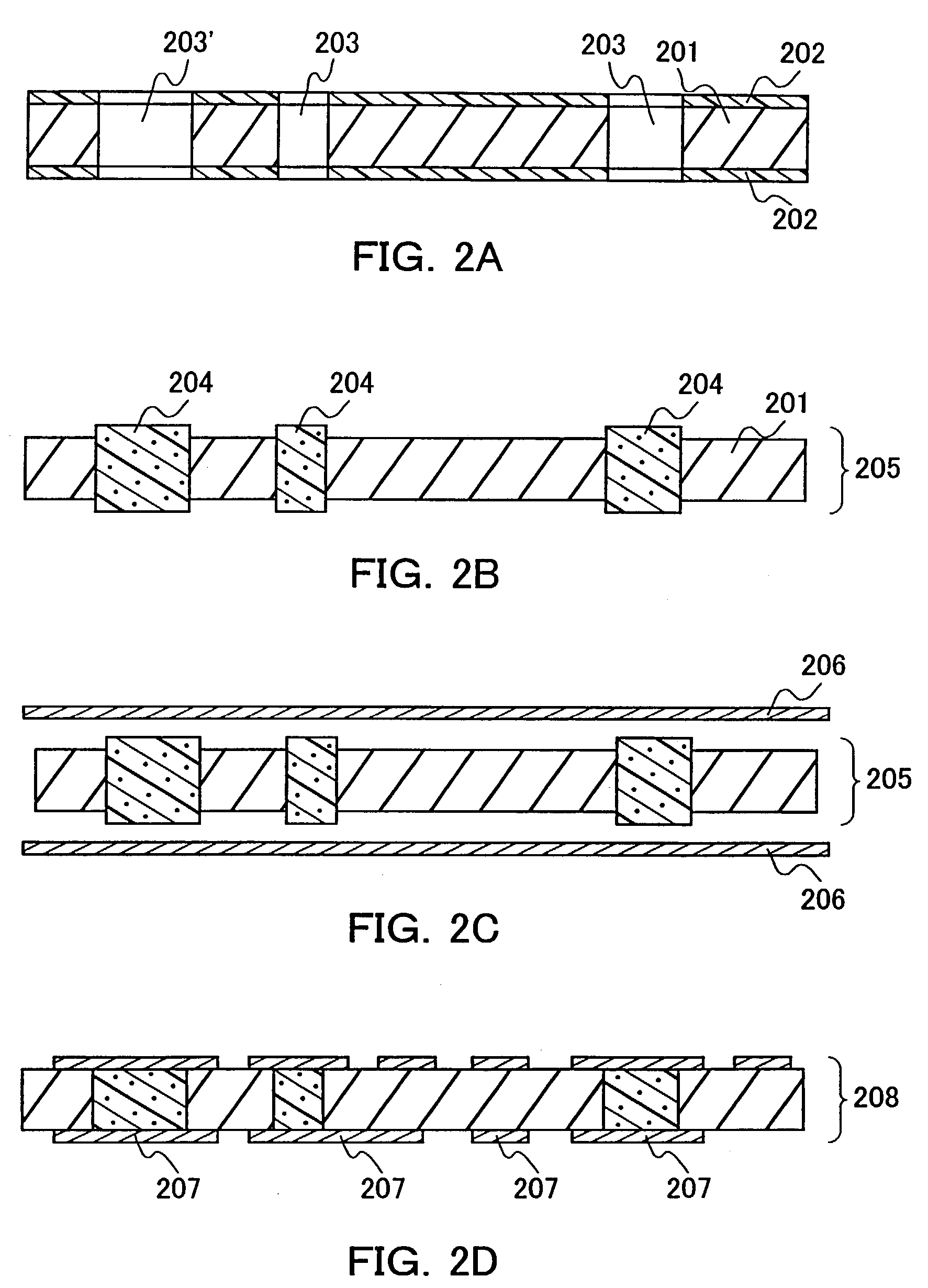
[0097]FIG. 6 is a schematic cross-sectional view showing a multilayered circuit board according to the second embodiment of the present invention. The multilayered circuit board of the present embodiment has a structure in which the circuit board described in the first embodiment is laminated on at least one surface of a core substrate formed of a compressible insulator base material. In this figure, a double-sided circuit board 401 of an aramid-epoxy substrate is used as the core substrate, and circuit boards 402 formed of a glass-epoxy base material described in the first embodiment are laminated on both sides of the core substrate.

[0098]The multilayered circuit board of the present embodiment can be produced as follows.

[0099]First, a double-sided circuit board is produced by using an aramid-epoxy prepreg. Cover films temporarily are attached by pressure onto both surfaces of the aramid-epoxy prepreg, and then through holes are formed. The through holes can be formed to have a dia...

third embodiment

[0104]FIG. 7 is a schematic cross-sectional view showing a multilayered circuit board according to the third embodiment of the present invention. The multilayered circuit board according to the present embodiment has a structure in which a circuit board 501 of the first or the second embodiment is used as a core substrate and a circuit board 502 with an insulator layer thinner than that of the core substrate is laminated on at least one surface of the core substrate. In a thinner insulator layer, it is possible to form finer inner via holes with lower resistance. This is because, even when the hole diameter is the same, a reduction in the length of the inner via hole, namely, the thickness of the insulator layer, decreases the connection resistance.

[0105]The following is a description of the case of using the four-layered circuit board of the second embodiment as the core substrate and a polyimide film as the insulator layer thinner than that of the core substrate.

[0106]The multilay...


PUM

PropertyMeasurementUnit
thicknessaaaaaaaaaa
diameteraaaaaaaaaa
thicknessaaaaaaaaaa

Abstract

A circuit board includes an electrical insulator layer formed of a reinforcer sheet with density distribution in its in-plane direction, an electrical conductor filled in a plurality of inner via holes provided in the electrical insulator layer in its thickness direction, and a wiring layer connected to the electrical conductor. The inner via holes provided in a high-density portion of the reinforcer sheet are formed to have a smaller cross-section than the inner via holes provided in a low-density portion of the reinforcer sheet. In this manner, it is possible to provide a circuit board that can achieve a high-density wiring and an inner via connection resistance with less variation, when a base material including a reinforcer sheet with density distribution in its in-plane direction such as a glass-epoxy base material is used for an insulator layer.

Description

CROSS REFERENCE TO RELATED DOCUMENT[0001]The present application is a Division of Application Ser. No. 10 / 045,344, filed on 25th Oct., 2001, now U.S. Pat. No. 6,558,780 B2, which claims the benefit of Japanese Application, JAPAN 2000-341646, filed on 9th Nov. 2000.BACKGROUND OF THE INVENTION[0002]1. Field of the Invention[0003]The present invention relates to a circuit board and a method for manufacturing the same. In particular, the present invention relates to a circuit board using a reinforcer sheet with density variations in its in-plane direction and a method for manufacturing the same.[0004]2. Description of Related Art[0005]In recent years, accompanying the reduction in size and weight and the improvement in function and performance of electronic equipment, there has been an increasing demand for low-cost multilayered circuit boards allowing a high density mounting of semiconductor chips such as large-scale integrated circuits (LSIs), in the field of not only industrial appli...

Claims


Application Information

Patent Timeline
Patent Type & Authority Patents(United States)
IPC IPC(8): H01K3/10H05K1/03H05K1/11H05K3/00H05K3/40H05K3/46
CPCH05K1/0366H05K3/4069Y10T428/24917H05K3/0032H05K3/0047H05K3/4614H05K3/4652H05K2201/0287H05K2201/029H05K2201/0355H05K2201/094H05K2203/1461Y10S428/901Y10T29/49155Y10T29/49165Y10T29/4913Y10T29/49126Y10T29/49128Y10T428/24802Y10T428/24322H05K1/115Y10T428/249953Y10T428/24994
Inventor SUZUKI, TAKESHINISHII, TOSHIHIROTOMEKAWA, SATORUECHIGO, FUMIO
Owner PANASONIC CORP
Why Eureka
Try Eureka