

Capacitance-type inertial detecting device
a sensor and capacitive technology, applied in the field of capacitive inertial sensor, can solve the problems of inherently limited manufacturing ratio of thickness h of the structure to the feasible gap g/sub>0 /sub>, increase in manufacturing cost, and inability to meet the requirements of detecting the effect of inertial motion, etc., to achieve the effect of reducing noise or non-linear output, reducing the sensitivity of the sensor, and increasing the sn ratio
- Summary
- Abstract
- Description
- Claims
- Application Information
AI Technical Summary
Benefits of technology
Problems solved by technology
Method used
Image

Examples
first embodiment
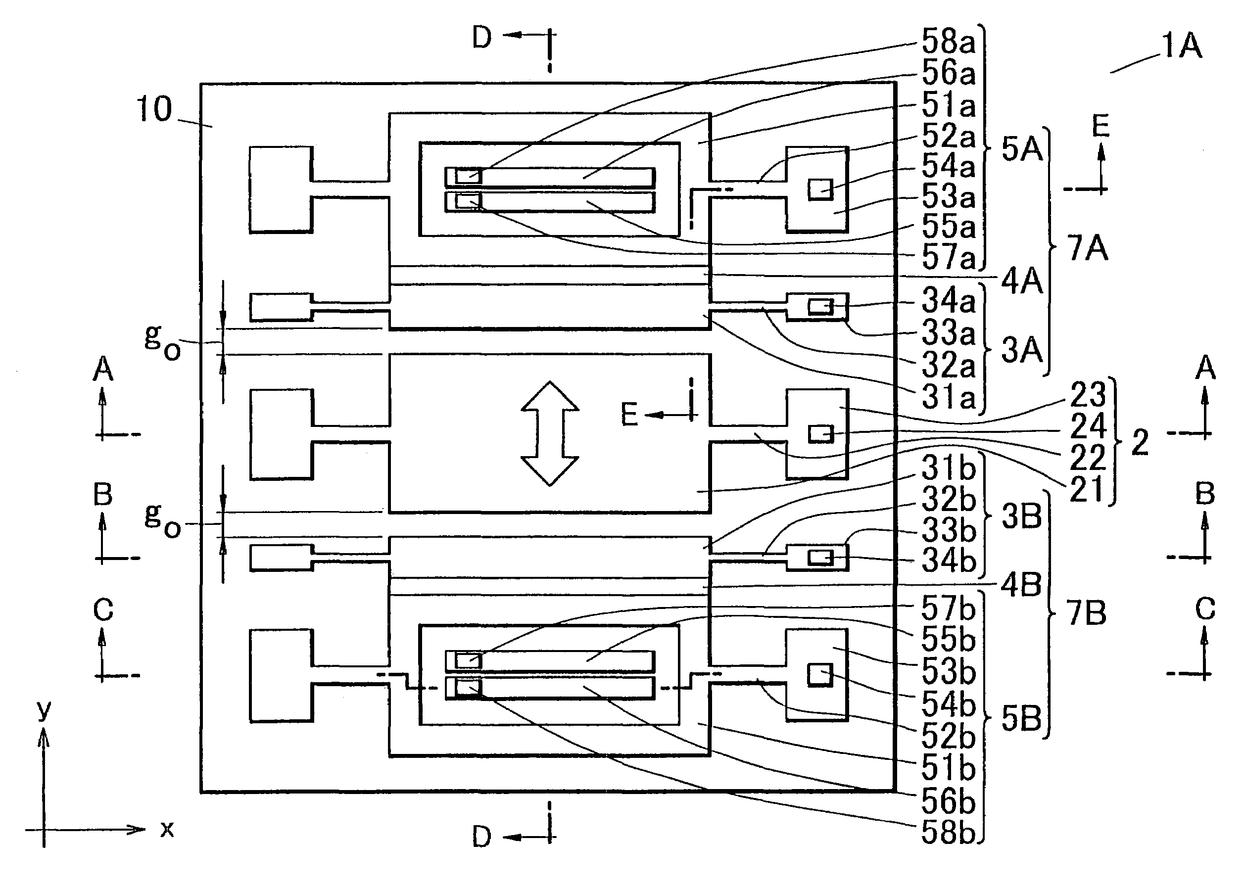
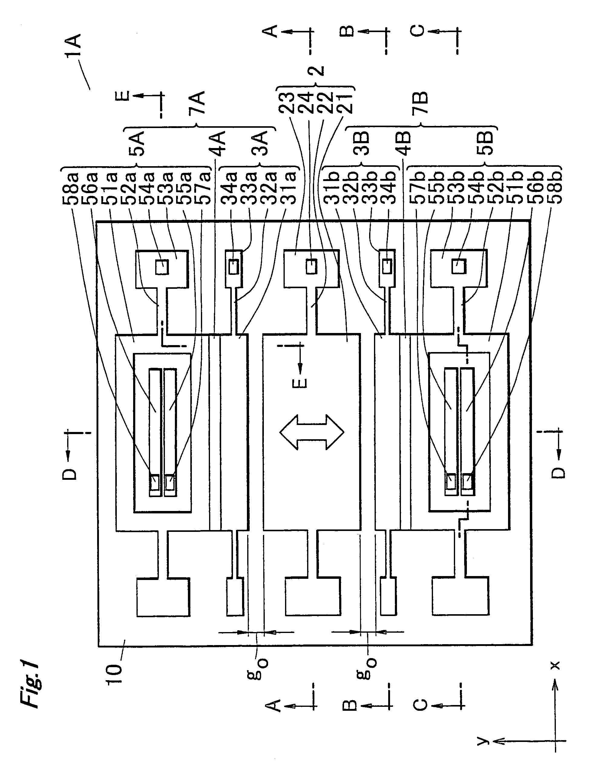
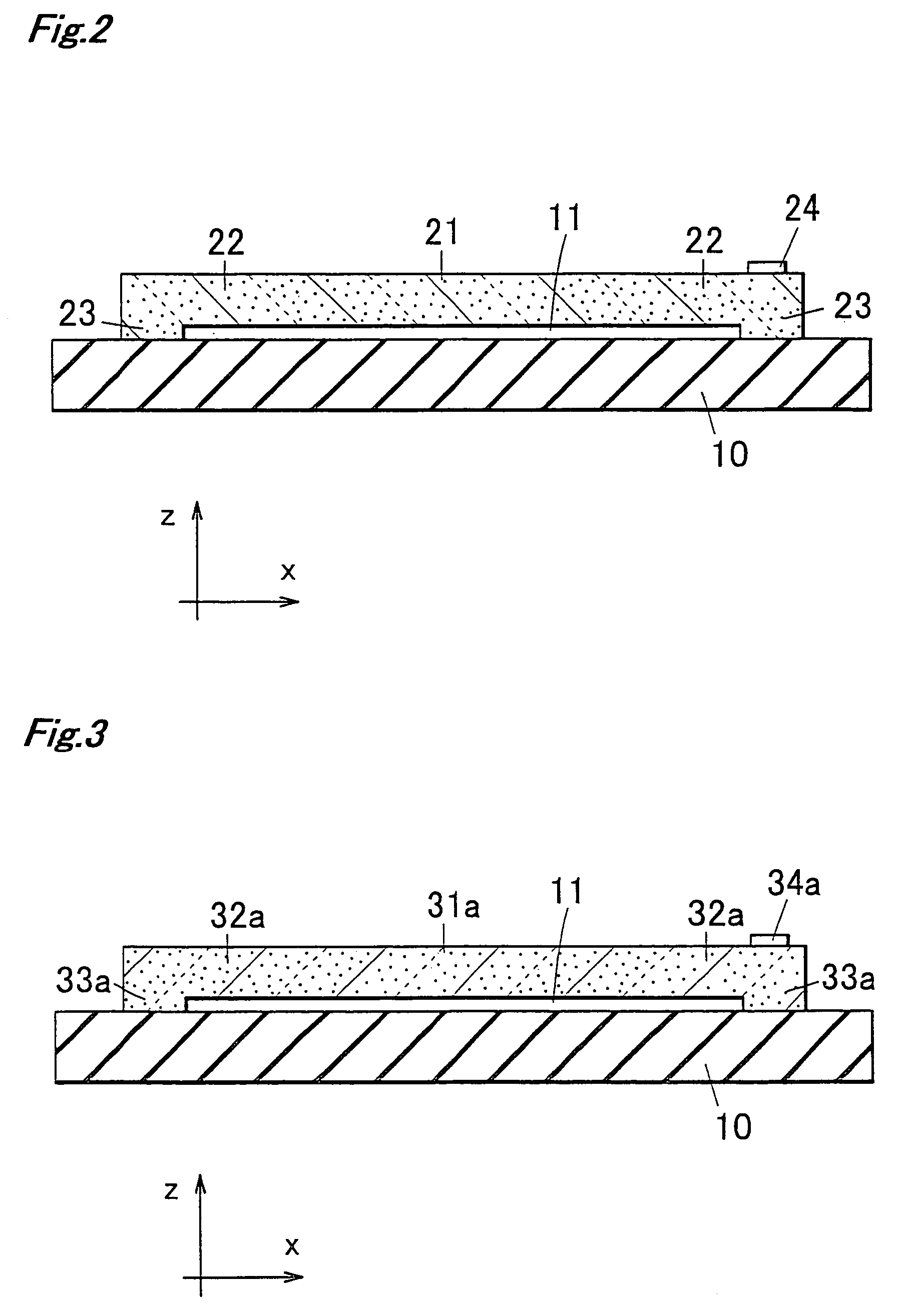
[0059]FIG. 1 is a schematic plan view showing the structure of a sensor element for a capacitive inertial sensor according to a first embodiment; FIG. 2 is an A—A cross sectional view of FIG. 1; FIG. 3 is a B—B cross sectional view of FIG. 1; FIG. 4 is a C—C cross sectional view of FIG. 1; and FIG. 5 is a D—D cross sectional view of FIG. 1.
[0060]Referring to FIG. 1, the sensor element includes a substrate 10, for example, having an electrically insulating layer at its surface, a displaceable unit 2 placed on the upper surface thereof, and a pair of detection units 7A and 7B, wherein the displaceable unit 2 is placed opposite to each of the pair of detection units 7A and 7B and separated by a specific gap from each of the detection units 7A and 7B. The substrate 10 may be a silicon substrate having an oxide film, a nitride film or the like at its surface, or an electrically insulating substrate such as a glass plate.
[0061]Referring to FIG. 2, the displaceable unit 2 includes a movabl...
second embodiment
[0101]FIG. 15 is a plan view showing the structure of a sensor element 1B for a sensor according to this embodiment; FIG. 16 is a partially enlarged plan view showing the structure of a drive unit 5C of the sensor element 1B; and FIG. 17 is a schematic diagram showing the configuration of a sensor I using the sensor element 1B.
[0102]The sensor element of the first embodiment as shown in FIG. 1 has a pair of fixed electrodes, which includes flat plate electrodes arranged in parallel, and a drive electrode (Gnd potential), in the drive unit. In such a case, electrostatic attraction generated between the drive electrode and the pair of fixed electrodes can be reversely proportional to the square of the gap; thus, the relationship between the displacement and the potential difference between the electrodes can be non-linear. In addition, a large displacement can cause a sticking phenomenon between the fixed electrode and the drive electrode. Therefore, for example, the drive unit may be...
third embodiment
[0111]FIG. 18 is a schematic plan view showing the structure of a sensor element 1C for a sensor according to this embodiment. The sensor element 1C may have the same structure as that of the sensor element 1A of the first embodiment, except that it has plural pairs of detection units in place of a pair of detection units. Referring to FIG. 18, the sensor element 1C includes a displaceable unit 120 and four pairs of detection units including first detection units 130A and 130B, second detection units 131A and 131B, third detection units 132A and 132B, and fourth detection units 133A and 133B, arranged on a substrate. The displaceable unit 120 includes a movable mass member 121 displaceable in the direction of inertial force, a pair of beams 122 which are each connected to the movable mass member 121 to support the member 121 in a space over the gap, a pair of anchors 124 which support the beams and are bonded to the substrate, and a terminal 123. The four pairs of detection units ar...
PUM
 Abstract
Description
Claims
Application Information