Capacitive sensor measurement method for discrete time sampled system for in-circuit test

a sensor measurement and in-circuit test technology, applied in the direction of electronic circuit testing, measurement devices, instruments, etc., can solve the problems of ac reference source limitation, open circuits are common defects in the manufacture of pcb assemblies, and the configuration and settling time of relays can take a significant amount of tim

Inactive Publication Date: 2006-02-14
AGILENT TECH INC
View PDF9 Cites 11 Cited by
  • Summary
  • Abstract
  • Description
  • Claims
  • Application Information

AI Technical Summary

Benefits of technology

[0014]The invention advantageously allows the use of digital stimulation sources due to the fact that it does not utilize specific phase information (which is unavailable for digital tester sources) to correlate the capacitively coupled signal with the source signal. Because the digital stimulation signal utilizes a known pattern, the sensed signal can be correlated with the stimulation signal based on pattern recognition rather than specific phase information. Another advantage of the invention is that by allowing the use of ubiquitously available digital stimulation sources normally used for functional test in the tester, the setup time for the acquisition of multiple capacitively sensed measurements is significantly decreased.
is that by allowing the use of ubiquitously available digital stimulation sources normally used for functional test in the tester, the setup time for the acquisition of multiple capacitively sensed measurements is significantly decreased.

Problems solved by technology

Open circuits are a common defect in the manufacture of PCB assemblies, typically occurring as a result of poor solder bonds, incomplete traces, and / or missing devices that are either never loaded onto the board or which fall off during the assembly process.
In large testers, the number of available AC reference sources may be limited.
As known in the art, the relay configuration and settling time can take a significant amount of time relative to the time required to obtain the capacitively coupled measurement.
Since a PCB can contain hundreds or thousands or more nets and net-to-component connections to be tested, this relay configuration procedure can prove to be too costly in terms of test time when only a limited number of AC sources are available for net stimulation.
However, because the digital sources generate no phase information, in the past digital sources have not been used to obtain capacitively sensed measurements because the digital sources cannot be phase synchronized with the capacitively coupled signal.

Method used


Image

  • Capacitive sensor measurement method for discrete time sampled system for in-circuit test
  • Capacitive sensor measurement method for discrete time sampled system for in-circuit test
  • Capacitive sensor measurement method for discrete time sampled system for in-circuit test

Examples


first embodiment

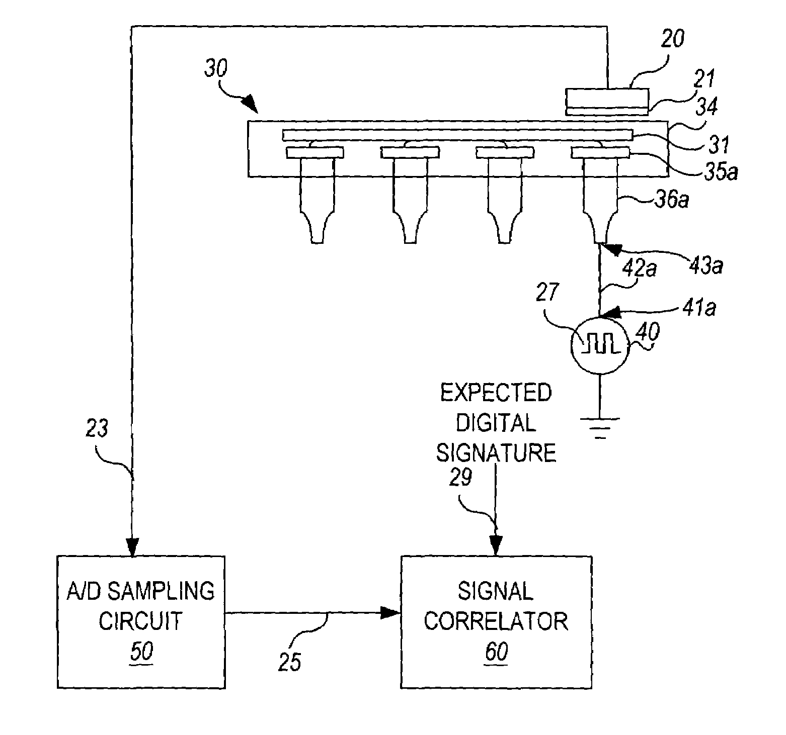
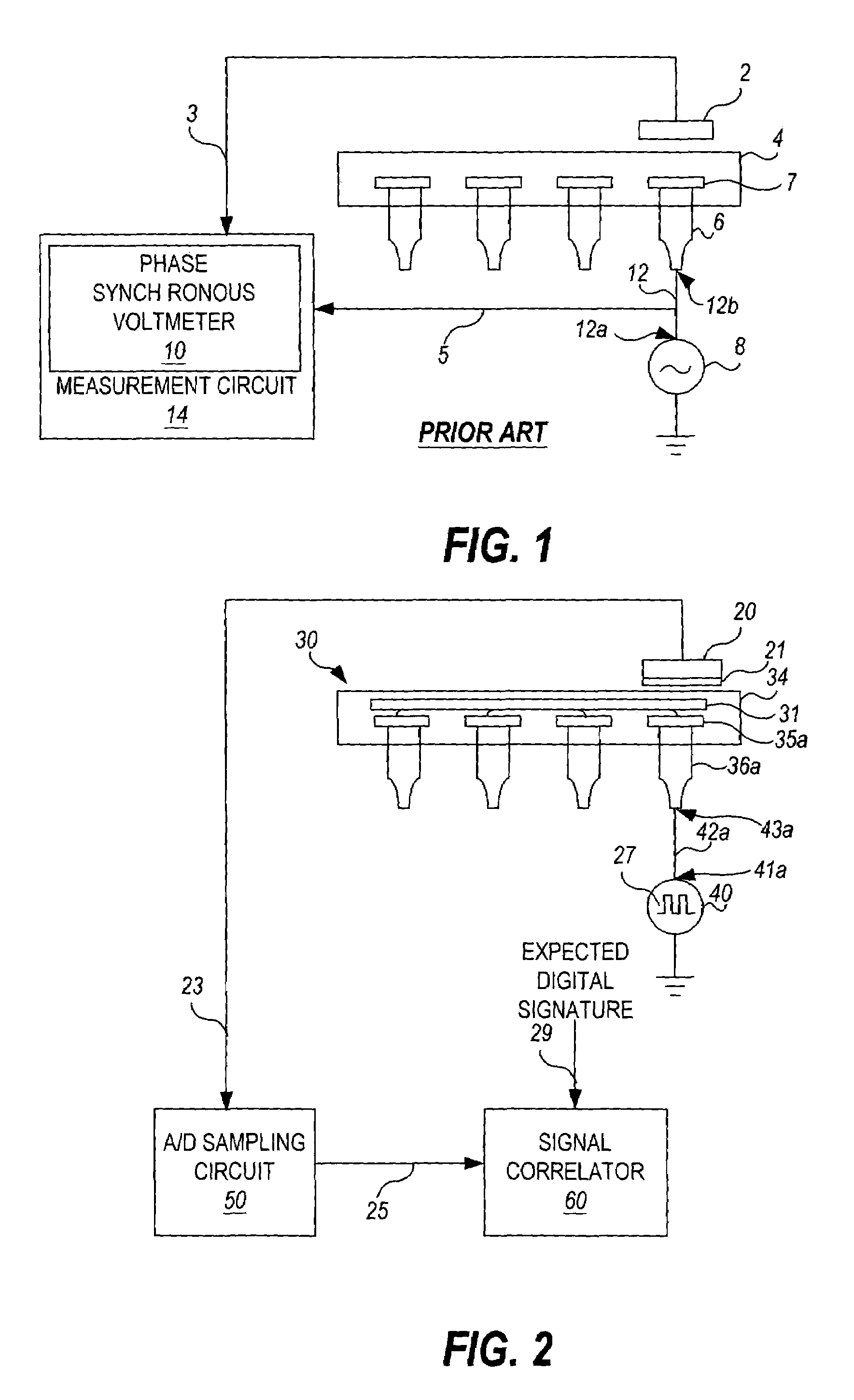
[0036]Turning now to the invention, FIG. 2 is a schematic block diagram of a test configuration for acquiring capacitively sensed measurements implemented according to the invention. In this configuration, a capacitive sensing probe 20 comprising a metallic electrode 21 is placed on top of the package 34 of an integrated circuit chip 30. A net 42a (which may be a wire, a trace, a solder bump, or any other known conductive material, and / or combination thereof) is characterized by a first end 41a connected to the output of an oscillating digital source 40 and a second end 43a connected to a pin 36a of the integrated circuit chip 30.

[0037]Digital square-wave source 40 generates a reference signal (or “stimulus”) 27. Analog-to-digital (A / D) sampling circuit 50 is connected to receive a capacitively coupled signal 23 sensed by probe 20. The sampling circuit 50 samples at least two times (2×) the frequency of the reference signal 27. In the preferred embodiment, the sampling rate is ten t...

second embodiment

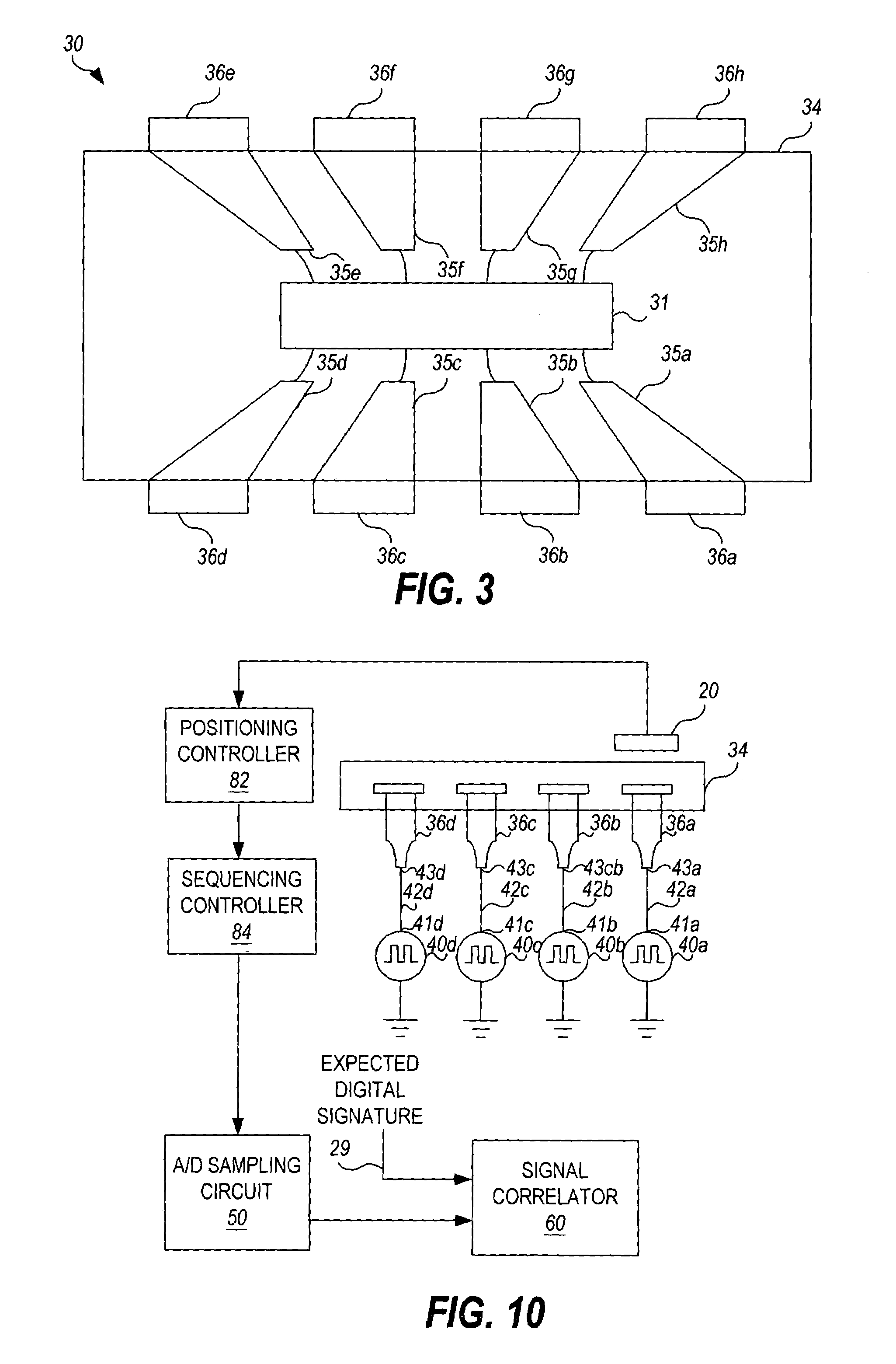
[0051]FIG. 10 is a schematic block diagram of a second embodiment test configuration for acquiring multiple capacitive sensor measurements implemented according to the invention. In this configuration, multiple nets 45a, 45b, 45c, 45d of interest are tested. In the example shown, each net 45a, 45b, 45c, 45d (which may be a wire, a trace, a solder bump, or any other known conductive material, and / or combination thereof) is characterized by a first end 41a, 41a, 41b, 41c, 41d connected to the output of a respective oscillating digital source 40a, 40b, 40c, 40d, and a second end 43a, 43b, 43c, 43d connected to a respective integrated circuit pin 36a, 36b, 36c, 36d.

[0052]In the embodiment of FIG. 10, the area of the metallic electrode plate 21 of the capacitive sensing probe 20 is sized to cover only a portion of the conductor 35a, 35b, 35c, 35d, 35e, 35f, 35g, 35h connected to a single pin 36a, 36b, 36c, 36d, 36e, 36f, 36g, 36h of the integrated circuit package 34.

[0053]FIG. 11 shows ...

third embodiment

[0054]FIG. 12 is a schematic block diagram of a third embodiment test configuration for acquiring multiple capacitive sensor measurements implemented according to the invention. In this configuration, multiple nets 42a–42h of interest are tested. In the example shown, each net 42a–42h (which may be a wire, a trace, a solder bump, or any other known conductive material, and / or combination thereof) is characterized by a first end 41a–41h respectively connected to the output of a respective oscillating digital source 40a–40h, and a second end 43a–43h respectively connected to a respective integrated circuit pin 36a–36h.

[0055]FIG. 13 shows a top cutaway view of the integrated circuit chip 30 and capacitive sensing probes 20a–20h of FIG. 12 (indicated by dashed lines). As illustrated, a different respective capacitive sensing probe 20a, 20b, 20c, 20d, 20e, 20f, 20g, 20h is respectively aligned over a different respective internal lead conductor 35a, 35b, 35c, 35d, 35e, 35f, 35g, 35h of ...


PUM


Abstract

Disclosed is a novel method and apparatus for acquiring multiple capacitively sensed measurements from a circuit under test. Multiple digital sources are respectively connected to stimulate multiple respective first ends of multiple respective nets of interest. Respective second ends of the multiple respective nets of interest are capacitively sensed. The respective capacitively coupled signals are digitally sampled and shift correlated with respective expected digital signatures. If a high level of correlation is found for a given net, the net is electrically intact; otherwise, the net is characterized by either an open or some other fault that prevents it from meeting specification.

Description

BACKGROUND OF THE INVENTION[0001]Obtaining electrical measurements from nodes of an electrical device via a capacitive sensing probe is often performed during the testing of a printed circuit board. As known in the art, capacitive sensing is a technique often used in determining the electrical connectivity of pins, nodes, traces, and other electrical conductors. See, for example, U.S. Pat. No. 5,696,431, Identification of Pin-Open Faults By Capacitive Coupling to Keirn et al., U.S. Pat. No. 5,498,964, Capacitive Electrode System for Detecting Open Solder Joints in Printed Circuit Assemblies, to Kerschner et al., U.S. Pat. No. 5,254,953 to Crook et al., U.S. Pat. No. 5,241,336 to Crook et al., and U.S. Pat. No. 5,357,209 to Crook et al., all of which are incorporated by reference herein for all that they teach.[0002]For purposes of clarity, the description herein will use the following terminology. As termed herein:[0003]A “net” is an electrically conductive path between two endpoint...

Claims


Application Information

Patent Timeline
Patent Type & Authority Patents(United States)
IPC IPC(8): G01R31/08G01R31/02G01R31/303G01R31/312
CPCG01R31/312
Inventor TESDAHL, CURTIS A.PEIFFER, RONALD J.
Owner AGILENT TECH INC
Why Eureka
Try Eureka