Reticle defect detection using simulation

a technology of defect detection and simulation, applied in the field of retinal defect detection, can solve the problems of not providing much information to determine the printability of defects, affecting the lithography process, and itself not providing sufficient information, so as to reduce the probability of operator error, reduce the required simulation processing, and reduce delays and costs

Inactive Publication Date: 2006-02-14
KLA TENCOR TECH CORP
View PDF6 Cites 23 Cited by
  • Summary
  • Abstract
  • Description
  • Claims
  • Application Information

AI Technical Summary

Benefits of technology

[0019]By virtue of the foregoing arrangement, the present invention can provide a user with additional information regarding an identified defect, and in particular, information such as how the defect is likely to print on the wafer. With this additional information, a user generally will be more likely to make an accurate assessment regarding the significance of the defect. As a result, the present invention often can help avoid unnecessary re-works and at the same time identify truly problematic defects earlier, there...

Problems solved by technology

The above-discussed defect detection methods thus provide reports of the defects of the reticle under examination, but do not provide much information to determine the printability of the defect.
That is, the defect report itself does not provide sufficient information to determine whether or not each of the defects is likely to cause negative impact on the lithography process or to adversely affect the device performance.
Determining defect printability in this manner generally is very time-consuming, inconsistent, and inaccurate because it relies purely on the human operator's experience and intuition.
Errors in evaluating defect printability can be costly.
If the defect would not in fact have printed as the operator predicted, such cleaning and repair int...

Method used


Image

  • Reticle defect detection using simulation
  • Reticle defect detection using simulation
  • Reticle defect detection using simulation

Examples


Embodiment Construction

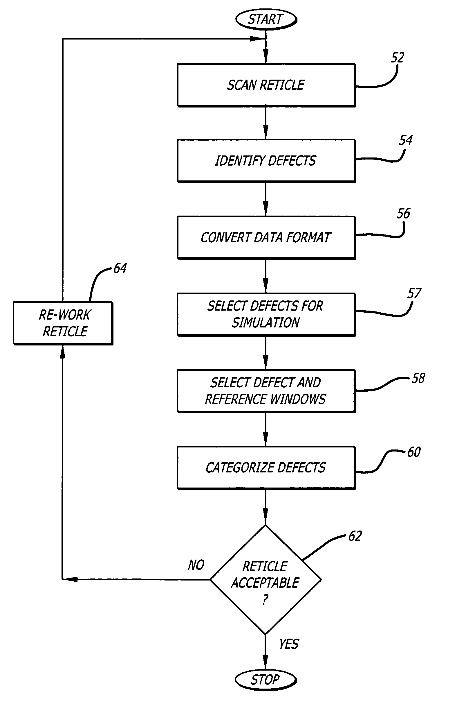
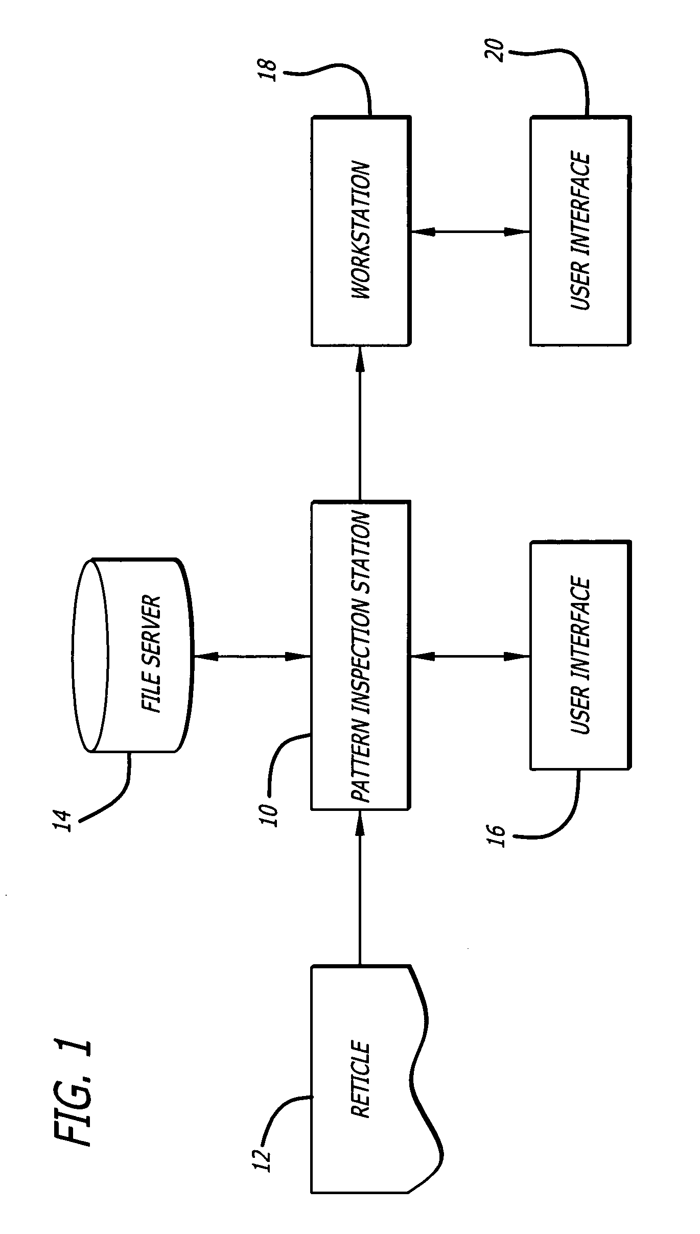
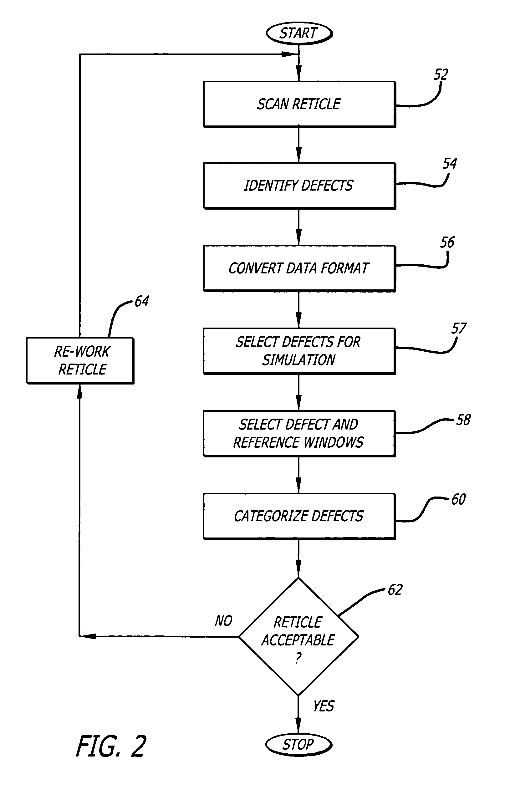
[0028]FIG. 1 illustrates a block diagram of a system implementing the present invention. Included in the system shown in FIG. 1 is a pattern inspection station 10, such as KLA-Tencor 200 or 300 series pattern inspection station. Included within pattern inspection station 10 is a scanner for inputting digital images of reticles, such as a reticle 12. Pattern inspection station 10 also includes program inspection steps for identifying defects, as defined in more detail below.

[0029]Connected to pattern inspection station 10 is file server 14, such as a KLA-Tencor 9X file server, for storing and retrieving image data files and program instruction steps. Also connected to pattern inspection station 10 is a user interface 16 which includes input devices such as a mouse and keyboard and output devices such as a CRT monitor and laser printer.

[0030]Under the control of inputs from user interface 16, as described in more detail below, pattern inspection station 10 transfers data files to work...


PUM


Abstract

Defects are detected in a reticle used in integrated circuit chip fabrication by obtaining digital image data corresponding to an image of the reticle. Typically, this is accomplished by scanning the reticle using a laser scanner. The digital image data are then processed according to predetermined criteria to identify defects. Such processing may include, for example, processing the digital image data in comparison to reference digital image data for the same or a similar portion of the reticle. Next, a response that would be produced if the reticle were to be utilized in a photolithographic system is simulated by processing the digital image data corresponding to the reticle.

Description

BACKGROUND OF THE INVENTION[0001]1. Field of the Invention[0002]The present invention relates to detection of defects in reticles used in the fabrication of integrated circuit chips. In particular, the invention concerns reticle defect detection using simulation of a photolithographic system.[0003]2. Description of the Prior Art[0004]Integrated circuits are made by photolithographic processes which use photomasks or reticles and an associated light source to project a circuit image onto a wafer. The light interacts with resist materials on the wafer to define various shapes and channels on the wafer. Then, after appropriate processing, the shapes and channels eventually define the electronic circuits on the wafer. Thus, reticles are used in the semiconductor manufacturing industry for the purpose of transferring photolithographic patterns onto a substrate, typically the wafer, during the manufacture of integrated circuits on the substrate. The wafer may be comprised of silicon, gall...

Claims


Application Information

Patent Timeline
IPC IPC(8): G06K9/00
CPCG01N21/95692G01N2021/95676G01N2021/95615
Inventor LOPEZ, DANIELSCHELLENBERG, FRANK
Owner KLA TENCOR TECH CORP
Why Eureka
Try Eureka