Plasma display panel and method for fabricating the same

a technology of plasma and display panels, which is applied in the manufacture of electrode systems, gas exhaustion means, electric discharge tubes/lamps, etc., can solve the problems of long life of ac types, difficulty in providing dc types with long life, and type requirements additional time, effort and cost, so as to improve the intensity, luminous efficiency and voltage margin, and reduce unnecessary power consumption.

Inactive Publication Date: 2006-02-21
PANASONIC CORP
View PDF30 Cites 24 Cited by
  • Summary
  • Abstract
  • Description
  • Claims
  • Application Information

AI Technical Summary

Benefits of technology

[0030]It is therefore an object of the present invention to provide a plasma display panel which can provide a high optical-output efficiency and high peak intensity and which can be driven with less maximum power consumption, and a method for fabricating the panel.
[0072]As described above, the plasma display panel according to the present invention can employ the prior-art driving method to improve the intensity, the luminous efficiency, and the voltage margin. In addition, the plasma display panel can reduce unnecessary power consumption on the bus electrode provided on the sustain electrode and the overall percentage of breaks in the sustain electrode to thereby provide improved fabrication yields. Accordingly, the plasma display panel provides great effects of reducing the power consumption of and improving the reliability of the display device employing the plasma display panel and greatly contributing to saving energy.
[0073]In addition, the present invention provides electrodes having a shape equivalent to comb-teeth, thereby making it possible to increase the luminous efficiency. Lattice-shaped ribs allow the electrodes between pixel cells to be closely spaced and thereby the effective opening portion of a pixel cell can be increased. This prevents the intensity from being reduced even when the comb-tooth-shaped electrodes are employed to increase the luminous efficiency. Furthermore, the sustain electrodes or the scan electrodes are connected to each other or shared between the pixel cells, thereby making it possible to provide further increased effective opening portion. This in turn makes it possible to provide further improved intensity and luminous efficiency. Furthermore, it is possible to reduce the resistance of electrodes, increase the voltage margin, improve the fabrication yields of the electrodes in the panel, and reduce the power consumption.

Problems solved by technology

Although the DC type has a simple structure, the electrodes are directly exposed to discharge environments and therefore wear out in a shorter period of time, thereby making it difficult to provide the DC type with long life.
In contrast, the AC type requires additional time, effort, and cost to form the insulating layer, however, the electrodes are covered with the insulating layer, thereby providing the AC type with long life.
However, as can be seen from the cross-sectional view of FIG. 3, there is a drawback, in outputting the light emitted from the phosphor 17 upwards in FIG. 55, that the bus electrode 13c present above the phosphor 17 provides an insufficient optical output efficiency.
Accordingly, there is a problem that this provides a low ratio of luminous intensity to the power input for light emission (hereinafter referred to as the luminous efficiency), resulting in an increased power consumption of a display device employing the plasma display panel.

Method used


Image

  • Plasma display panel and method for fabricating the same
  • Plasma display panel and method for fabricating the same
  • Plasma display panel and method for fabricating the same

Examples


fifth embodiment

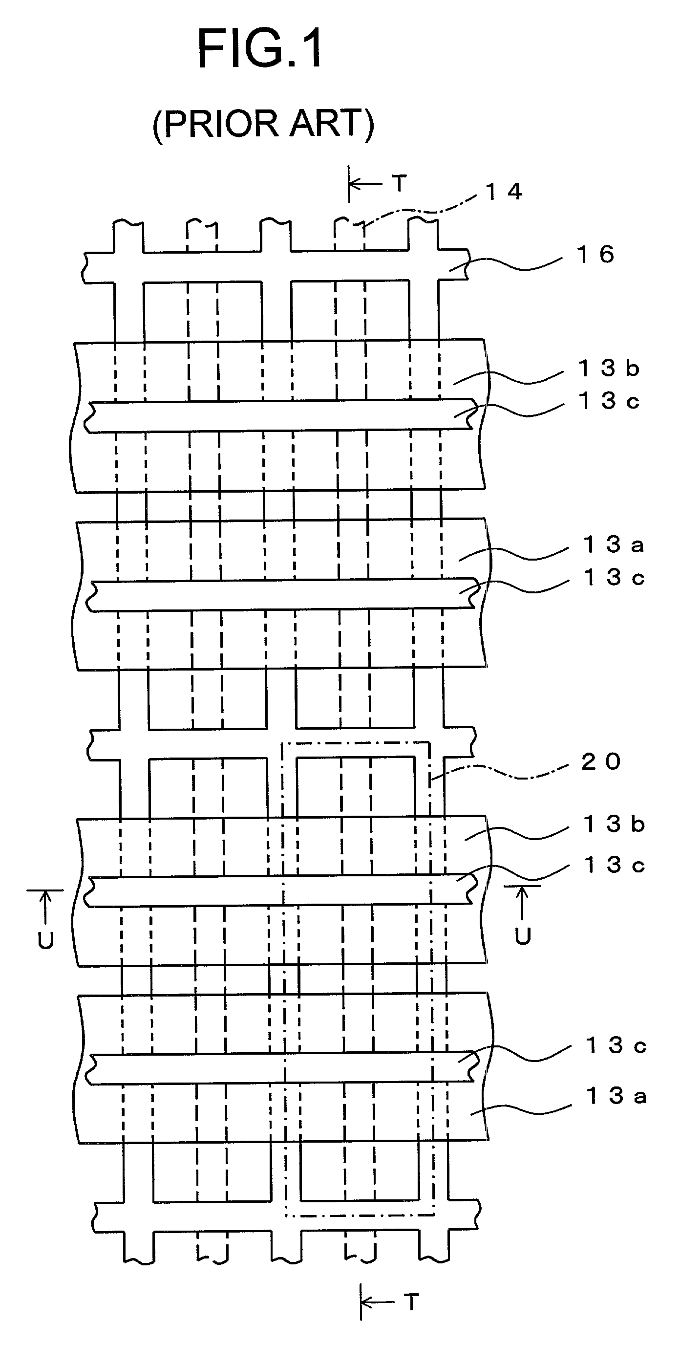
[0171]Now, a fifth embodiment of the present invention is described below. FIG. 16 is a perspective view illustrating a second insulating substrate 12 of a plasma display panel according to the fifth embodiment of the present invention. FIG. 17 is a plan view illustrating the plasma display panel according to the fifth embodiment of the present invention. In this embodiment, rib projections 53 are formed to extend in either direction from the intersections of the lattice-shaped ribs 16 in parallel to the direction of the column electrodes. As shown in FIG. 17, this allows the scan-side bus electrode 13e and the sustain-side bus electrode 13d to be separated from each other between neighboring pixel cells. The method for fabricating the plasma display panel according to this embodiment is the same as that of the fourth embodiment.

[0172]Even with projections residing at the intersections of the lattice-shaped ribs, the rib projections 53 allow the scan-side bus electrode 13e and the s...

seventh embodiment

[0176]Now, a seventh embodiment according to the present invention is described below. FIG. 19 is a plan view illustrating a plasma display panel according to the seventh embodiment of the present invention. In this embodiment, like the sixth embodiment shown in FIG. 18, the lattice-shaped rib 16 is formed on top of the second insulating substrate 12, and rib recesses 54 are formed on the intersection of the ribs 16. Additionally, in this embodiment, as in the embodiment shown in FIG. 7, there are formed the sustain electrode 13a, the scan electrode 13b, the sustain-side bus electrode 13d, and the scan-side bus electrode 13e. This embodiment also has the rib recesses 54 on top of the intersections of the ribs 16 to provide flow paths for a gas to be exhausted to a vacuum, thereby making it possible to easily perform exhaustion by the same encapsulating and exhausting method as the prior-art method. Incidentally, it is possible to fabricate the plasma display panel according to this ...

eighth embodiment

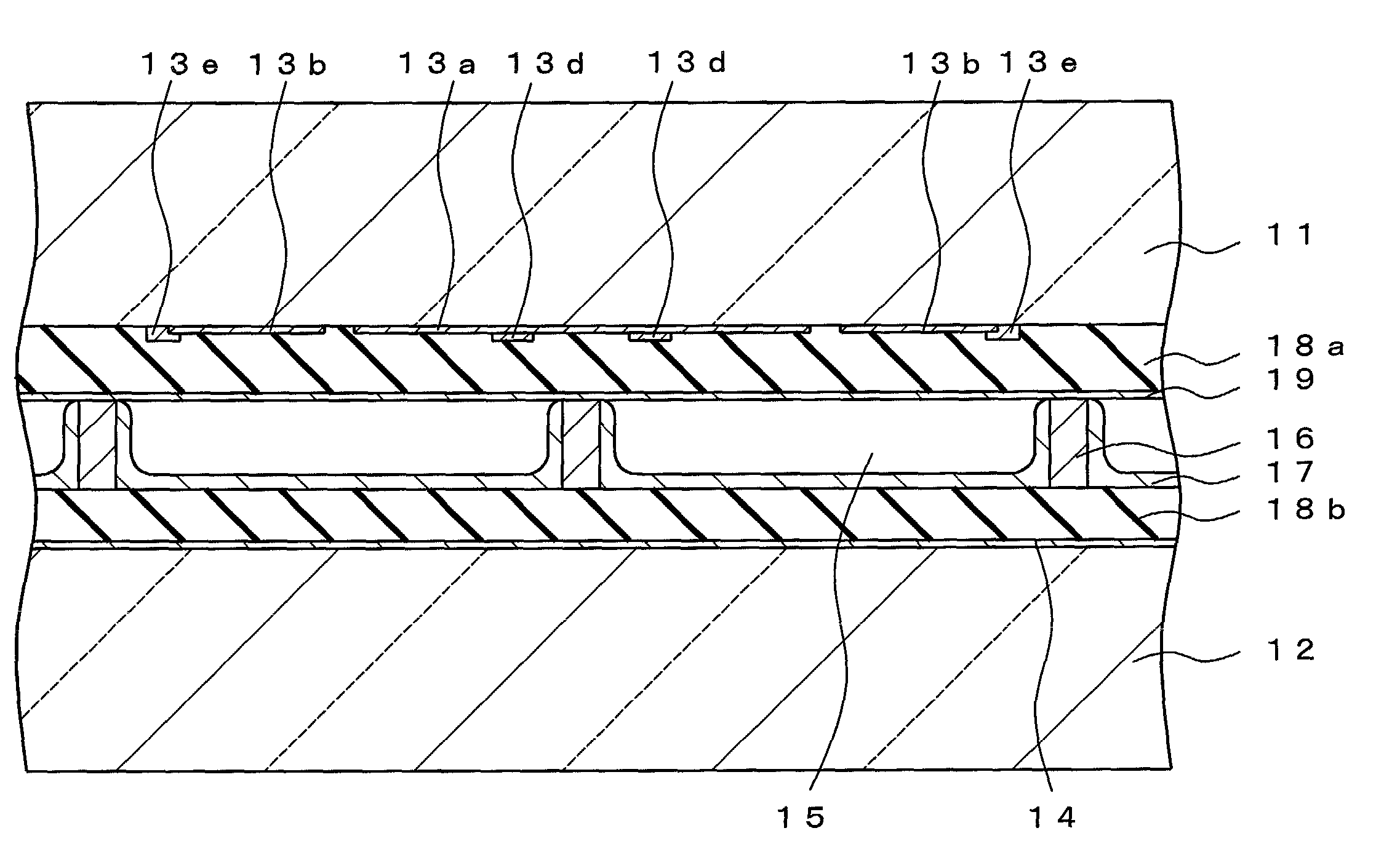
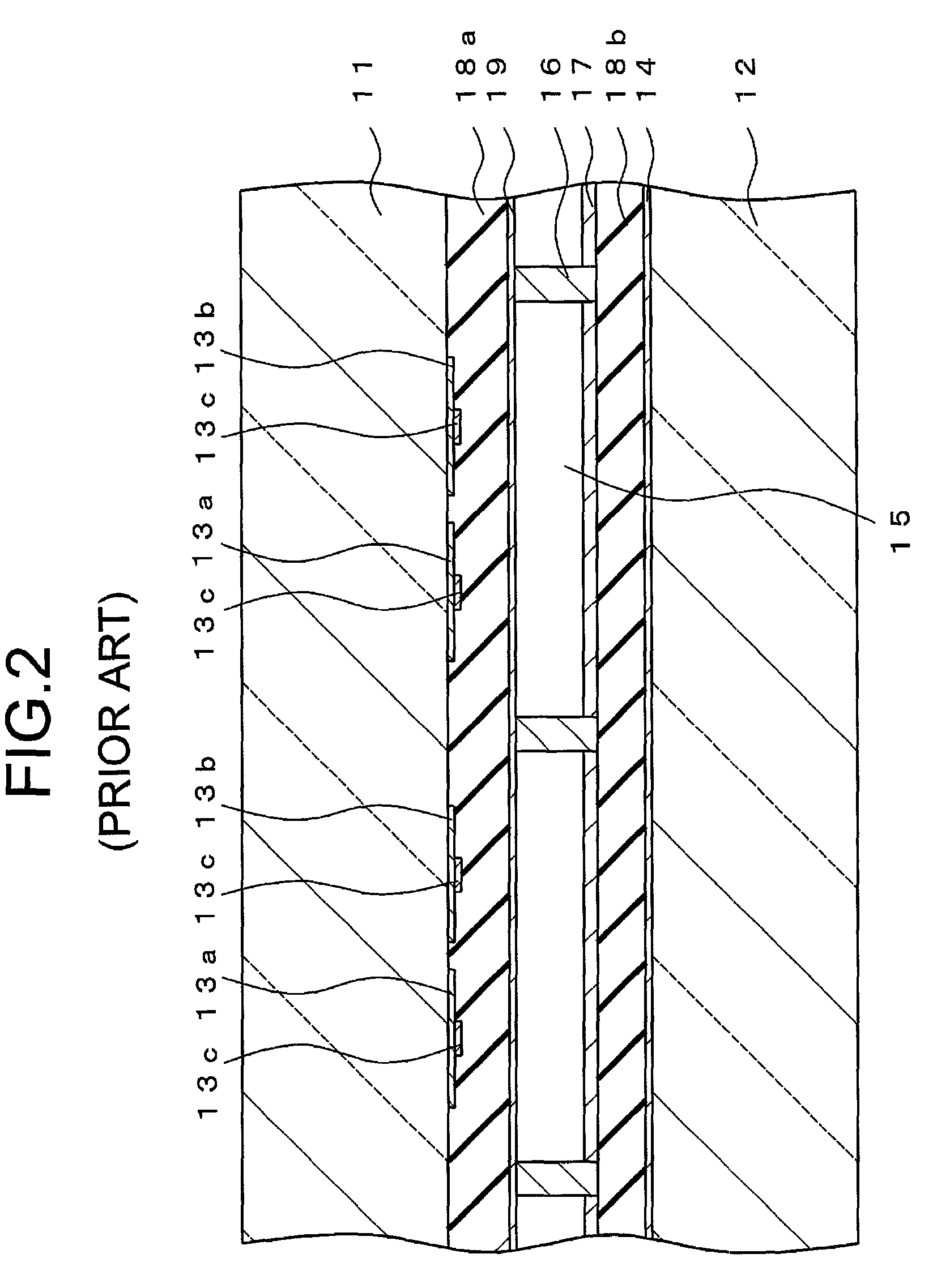
[0179]Now, an eighth embodiment according to the present invention is described below. FIG. 20 is a plan view illustrating a plasma display panel according to the eighth embodiment of the present invention. FIG. 21 is a cross-sectional view taken along line F—F of FIG. 20 and FIG. 22 is a cross-sectional view taken along line G—G of FIG. 20. The same components of FIGS. 20 to 22 as those of FIGS. 7 to 9 are provided with the same reference symbols and will not be repeatedly explained in detail.

[0180]This eighth embodiment is different from the first embodiment in having horizontal barrier walls 23. In this embodiment, the horizontal barrier wall 23 is formed on top of the insulating layer 18a of the first insulating substrate 11. The horizontal barrier wall 23 has a height of 2 to 50 μm and desirably 5 to 30 μm. In addition, the horizontal barrier wall 23 is located between the sustain-side bus electrodes 13d and between the scan-side bus electrodes 13e.

[0181]It is possible to form...


PUM


Abstract

Ribs for defining pixel cells are formed in the shape of a lattice, and sustain electrodes and scan electrodes are disposed near the ribs. The electrodes are spaced apart in each pixel cell, and the sustain electrode and the scan electrode are each cut away between pixel cells arranged in the row direction to provide each pixel cell with individually separated electrodes. In addition, between pixel cells adjacent to each other in the row direction, the sustain electrodes and the scan electrodes are connected to each other by means of a sustain-side bus electrode and a scan-side bus electrode, respectively. This makes it possible to provide a high luminous efficiency.

Description

BACKGROUND OF THE INVENTION[0001]1. Field of the Invention[0002]The present invention relates to plasma display panels which are employed as an image display device for use with information terminal devices, personal computers, televisions or the like. More particularly, the present invention relates to a plasma display panel and its fabrication method which make it possible to provide a higher peak intensity and less maximum power consumption for a plasma display panel, having a large capacity and a high resolution, than prior-art panels and methods.[0003]2. Description of the Related Art[0004]Plasma display panels have such advantages that they have a simple construction, facilitates the provision of a large screen, and can employ inexpensive glass materials, which are widely used for glass windows or the like, as substrates for constituting the display panel.[0005]A plasma display panel employs two transparent insulating substrates formed of such a glass material, each transparen...

Claims


Application Information

Patent Timeline
Patent Type & Authority Patents(United States)
IPC IPC(8): H01J17/49H01J9/26H01J9/18H01J9/385H01J11/12H01J11/14H01J11/22H01J11/24H01J11/26H01J11/32H01J11/34H01J11/36H01J11/38H01J11/48H01J11/54H01J17/04
CPCH01J11/12H01J11/24H01J11/32H01J11/36H01J2211/361H01J2211/245H01J2211/323H01J2211/326H01J9/02
Inventor SANO, YOSHIOAIBARA, NOBUMITSUYANAI, YOSHIAKIAKIYAMA, TOSHIYUKIOKAMOTO, TETSUMASAYANAGIDA, KAZUAKITATENO, HIROKAZUHIRANO, NAOTOTANAKA, YOSHITONAKAMURA, TADASHINUNOMURA, KEIJI
Owner PANASONIC CORP
Why Eureka
Try Eureka