Nonreflective waveguide terminator and waveguide circuit

a waveguide terminator and waveguide technology, applied in the direction of electrical equipment, basic electric elements, electromagnetic wave modulation, etc., can solve the problems of waveguide terminator, high production cost, waveguide terminator, etc., and achieve low production cost and good high-power tolerant performance

Inactive Publication Date: 2006-02-21
MITSUBISHI ELECTRIC CORP
View PDF27 Cites 18 Cited by
  • Summary
  • Abstract
  • Description
  • Claims
  • Application Information

AI Technical Summary

Benefits of technology

[0011]The present invention is made in order to solve the above problems. It is an object of the present invention to provide a small and light nonreflective waveguide terminator which has good high-power tolerant performance and which is produced at a low production cost.

Problems solved by technology

Accordingly, the nonreflective waveguide terminator in FIG. 16 has a problem in that the length of the electromagnetic-wave absorbing plates 3 must be increased in order to obtain a predetermined reflection level or less, even if it is more than enough for the length required for high-power tolerant performance such as heat radiation performance.
Also, the nonreflective waveguide terminator in FIG. 17 suffers from a problem of high production costs because it is difficult to perform processing of the tapered electromagnetic wave absorber 4.

Method used


Image

  • Nonreflective waveguide terminator and waveguide circuit
  • Nonreflective waveguide terminator and waveguide circuit
  • Nonreflective waveguide terminator and waveguide circuit

Examples


first embodiment

[0033]A first embodiment of the present invention is described below with reference to the accompanying drawings.

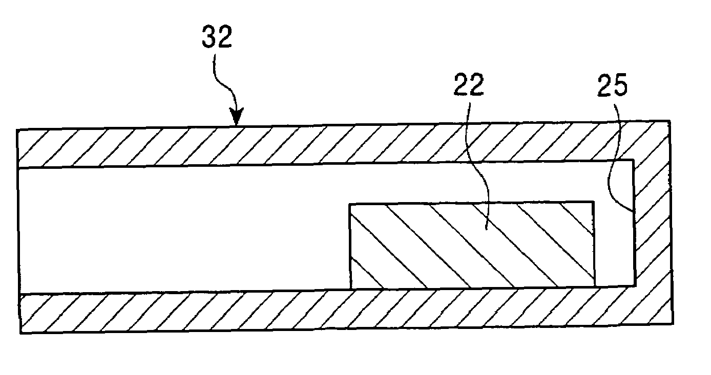
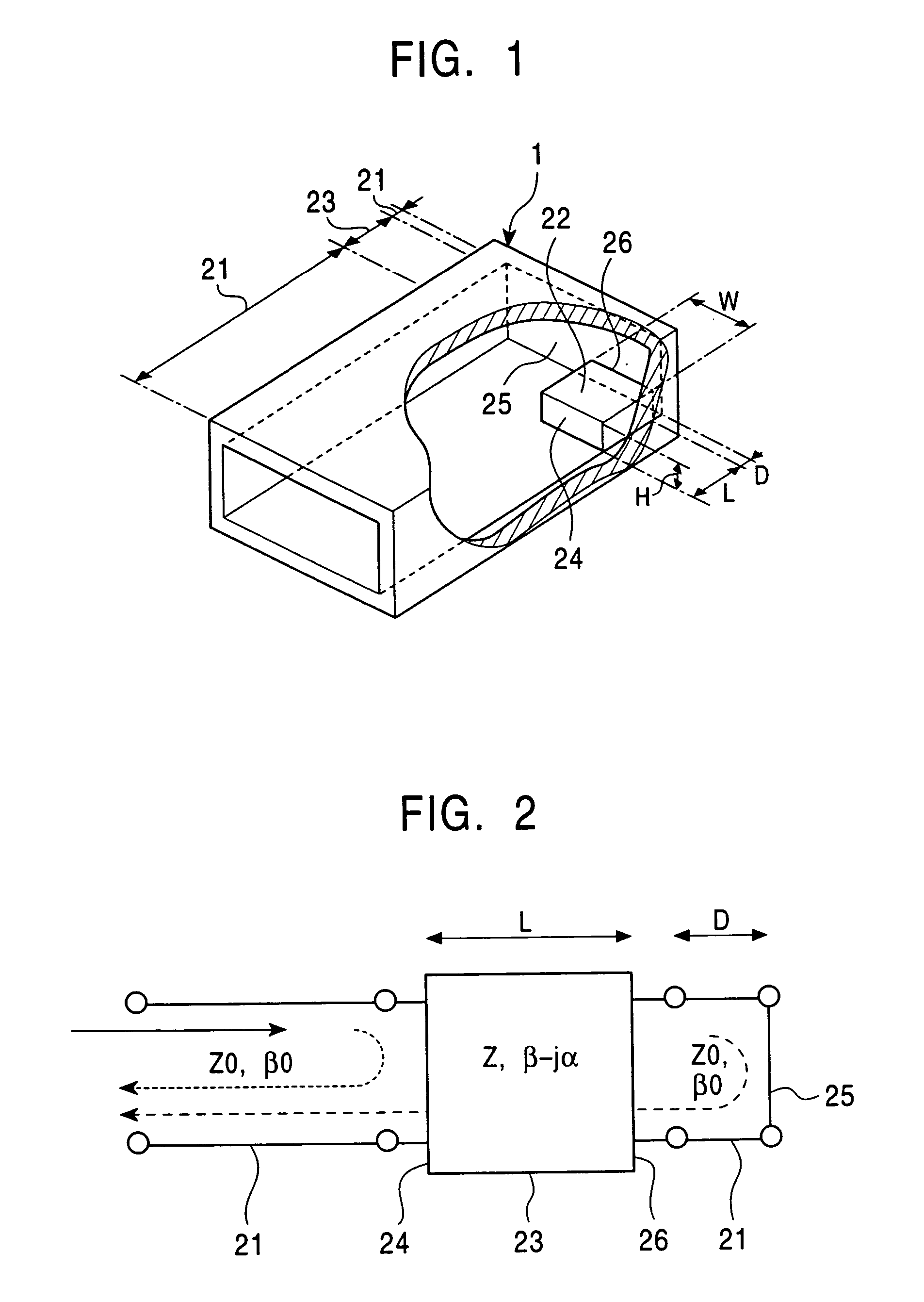
[0034]FIG. 1 shows a rectangular waveguide 1 having one short-circuited end, and a parallelepiped electromagnetic wave absorber 22. The rectangular waveguide 1 can be divided into rectangular waveguide portions 21 where the electromagnetic wave absorber 22 is not provided along the radio-wave traveling direction, and a rectangular waveguide portion 23 where the electromagnetic wave absorber 22 is provided. The electromagnetic wave absorber 22 is disposed on a wall surface perpendicular to the electric field in the rectangular waveguide 1. For the electromagnetic wave absorber 22, material obtained by using epoxy resin to bind metal powder such as iron powder, and ceramic material such as ferrite are used. The electromagnetic wave absorber 22 is fixed to the wall surface of the rectangular waveguide 1 by using, for example, a silicon-rubber-based adhesive.

[0035]The rectang...

second embodiment

[0049]Although the first embodiment only describes functional parts of the nonreflective waveguide terminator, the nonreflective waveguide terminator has similar advantages if it is formed in an integrated manner with a waveguide portion having another function. By way of example, FIG. 11 shows an output power combining circuit 69 including four amplifying elements 63 used as microwave amplifiers. The output power combining circuit 69 includes input ports 65 such as microstrip lines, the amplifying elements 63 such as microwave semiconductors, conversion circuits 64 between output transmission lines of the amplifying elements 63, and a waveguide, a waveguide combining circuit 61 such as a 3-dB-90-degree branch line hybrid, and an output terminal 66 of the waveguide. The waveguide circuits having functions are constituted by waveguide circuit parts 67 and 68 which are divided on an E plane.

[0050]FIGS. 12, 13, and 14 are illustrations of the operation of the second embodiment of the p...


PUM


Abstract

A nonreflective waveguide terminator includes a waveguide portion and an electromagnetic wave absorber. The portion has a rectangular opening in a plane perpendicular to a radio-wave propagation direction. The portion has one open end in the direction and the other end closed by a terminating metal internal wall. The portion has a radio-wave propagation space surrounded by first and second metal internal walls parallel to a radio-wave electric field, and third and fourth metal internal walls perpendicular to the field. The exterior shape of the absorber is a parallelepiped. The absorber has a rear-end surface positioned at a predetermined distance from the terminating wall and parallel to the terminating wall or is provided against the terminating wall. The surface of the absorber having the largest rectangular area is on the third or the fourth metal internal wall.

Description

BACKGROUND OF THE INVENTION[0001]1. Field of the Invention[0002]The present invention relates to a nonreflective waveguide terminator and a waveguide circuit which transmit microwave and millimeter-wave signals.[0003]2. Description of the Related Art[0004]FIG. 16 is a perspective view showing the structure of a nonreflective waveguide terminator disclosed in, for example, Japanese Unexamined Patent Application Publication No. 5-243817. In a rectangular waveguide 1 having one short-circuited end, electromagnetic-wave absorbing plates 3 for absorbing a high frequency magnetic field are disposed on wall surfaces 2 which are parallel to an electric field inside the rectangular waveguide 1.[0005]FIG. 17 is a perspective view showing the structure of a nonreflective waveguide terminator disclosed in Japanese Unexamined Patent Application Publication No. 5-243817. In a rectangular waveguide 1 having one short-circuited end, a tapered electromagnetic-wave absorber is disposed in the center ...

Claims


Application Information

Patent Timeline
Patent Type & Authority Patents(United States)
IPC IPC(8): H01P1/00H01P1/26
CPCH01P1/264
Inventor ASAO, HIDEKIYOSHINO, YUKITSUGUHENMI, KAZUHISAOOHASHI, HIDEYUKITAHARA, YUKIHIROOGAWA, HIDEOYONEDA, NAOFUMIMUKUDA, MUNEAKI
Owner MITSUBISHI ELECTRIC CORP
Why Eureka
Try Eureka