

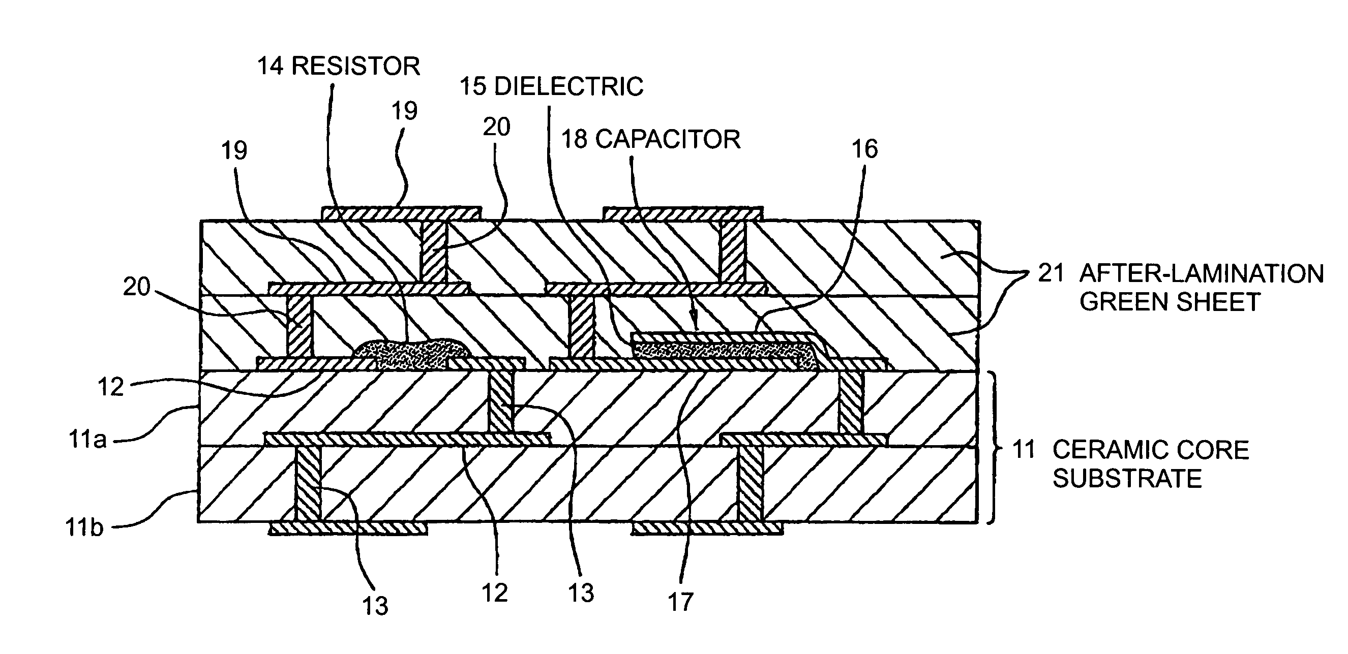
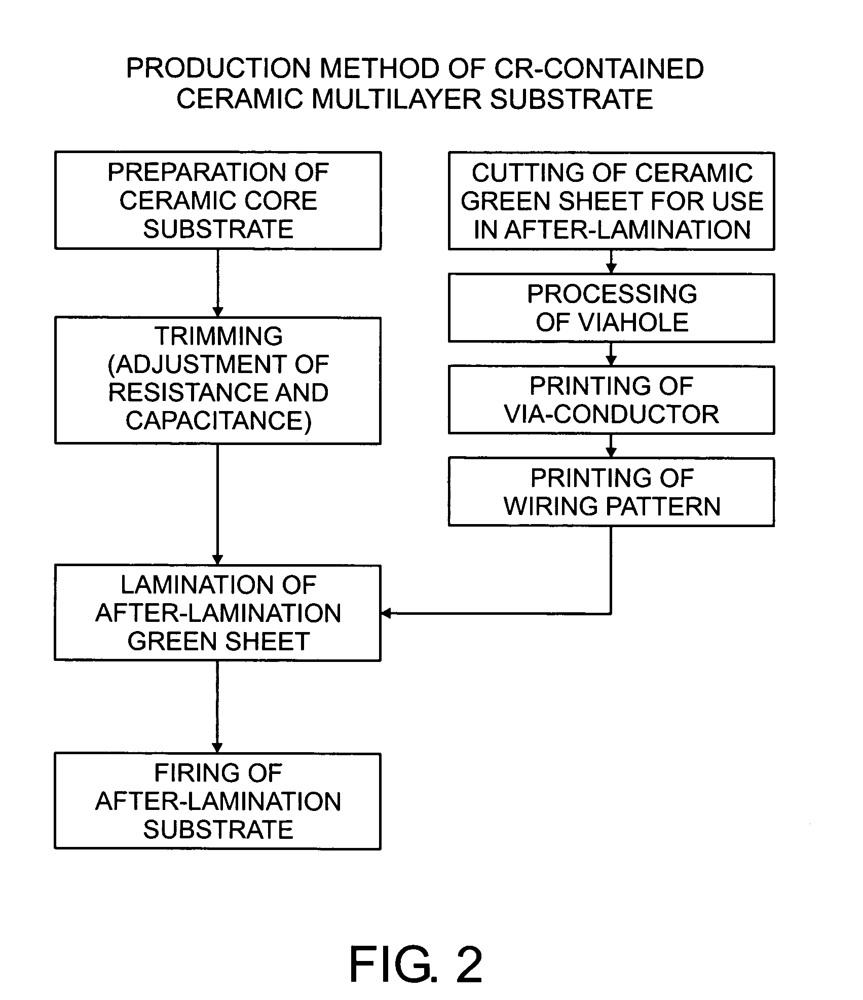
Method of producing ceramic multilayer substrate
a multi-layer substrate and ceramic technology, applied in the direction of structural fixed capacitor combination, cell components, electrochemical generators, etc., can solve the problems of reducing and affecting the mechanical strength of the ceramic core substrate. , to achieve the effect of enhancing the mechanical strength reducing the size and enhancing the wiring density of the ceramic core substra
- Summary
- Abstract
- Description
- Claims
- Application Information
AI Technical Summary
Benefits of technology
Problems solved by technology
Method used
Image

Examples
example
[0047]The inventors produced CR ceramic multilayer substrates according to the production method of this embodiment under different conditions. The variation of the resistance of the contained resistors and that of the capacitance of the contained capacitors were measured. Table 1 shows the measurements.
[0048]
TABLE 1FiringFiringMaterial fortemperatureMaterials forMaterialtemperature forDispersion ofDispersion ofceramicfor ceramiccontainedFiring condition forfor after-after-resistance ofcapacitancecorecoreresistor andcontained resistorlaminationlaminationcontainedof containedNo.substratesubstratecapacitorand capacitorgreen sheetsubstrateresistorcapacitorExample1A1900° C.R1Simultaneous firingA3700° C.±0.2%—2A1900° C.C1After-firingA3700° C.—±0.1%3A1900° C.R1, C1After-firingA3700° C.±0.3%±0.2%4A2900° C.R2After-firingA3700° C.±0.3%—5A2900° C.C2Simultaneous firingA3700° C.—±0.2%Comparative6A1900° C.R1Simultaneous firingA1900° C. ±22%—Example7A1900° C.C1After-firingA1900° C.— ±25%
[0049]In ...
PUM
| Property | Measurement | Unit |
|---|---|---|
| temperature | aaaaa | aaaaa |
| temperature | aaaaa | aaaaa |
| temperature | aaaaa | aaaaa |
Abstract
Description
Claims
Application Information