Differential amplifier circuitry formed on semiconductor substrate with rewiring technique

a technology semiconductor substrate, which is applied in the direction of amplifiers with min 3 electrodes or 2 pn junctions, amplifiers with semiconductor devices/discharge tubes, solid-state devices, etc., can solve the problems of deteriorating distortion characteristics of differential amplifier circuitry, and affecting the performance of amplifiers. , to achieve the effect of improving distortion characteristics and gains, and reducing characteristic deterioration

Inactive Publication Date: 2008-06-03
PANASONIC CORP
View PDF3 Cites 1 Cited by
  • Summary
  • Abstract
  • Description
  • Claims
  • Application Information

AI Technical Summary

Benefits of technology

[0009]It is an essential object of the present invention to solve the above-mentioned problems, and to provide differential amplifier circuitry and a radio communication apparatus that is capable of improving the distortion characteristics and gains, and has less characteristic deterioration due to signal interference between the differential amplifier circuitry and the other circuits formed on the same semiconductor substrate, as compared with the differential amplifier circuitry according to the prior art.
[0017]According to the differential amplifier circuitry and the radio communication apparatus according to the present invention, the distortion characteristics and gains can be improved, and characteristic deterioration due to signal interference between the differential amplifier circuitry and the other circuits formed on the same semiconductor substrate can be reduced, as compared with the prior art differential amplifier circuitry.

Problems solved by technology

Thus, a problem is created in that the higher-harmonic wave interferes with input signals and deteriorates distortion characteristics of the differential amplifier circuitry.
An additional problem is created in that the resistors 104 and 105 for biasing the bases of the transistors Q1 and Q2 attenuate the input signals, which causes a gain reduction.
Furthermore, in the case of forming the high-frequency differential amplifier circuitry on one chip with a modem circuit part and a frequency synthesizer part, there is still a further problem in that signals from the respective circuits interfere with one another via a semiconductor substrate, which causes characteristic deterioration such as generation of spurious signals and deterioration of noise and the like.
Otherwise, carrier leakage might occur when a local oscillation signal, inputted to a modulator, directly leaks into the transmission driver amplifier, which causes deterioration of modulation accuracy.

Method used


Image

  • Differential amplifier circuitry formed on semiconductor substrate with rewiring technique
  • Differential amplifier circuitry formed on semiconductor substrate with rewiring technique
  • Differential amplifier circuitry formed on semiconductor substrate with rewiring technique

Examples


first preferred embodiment

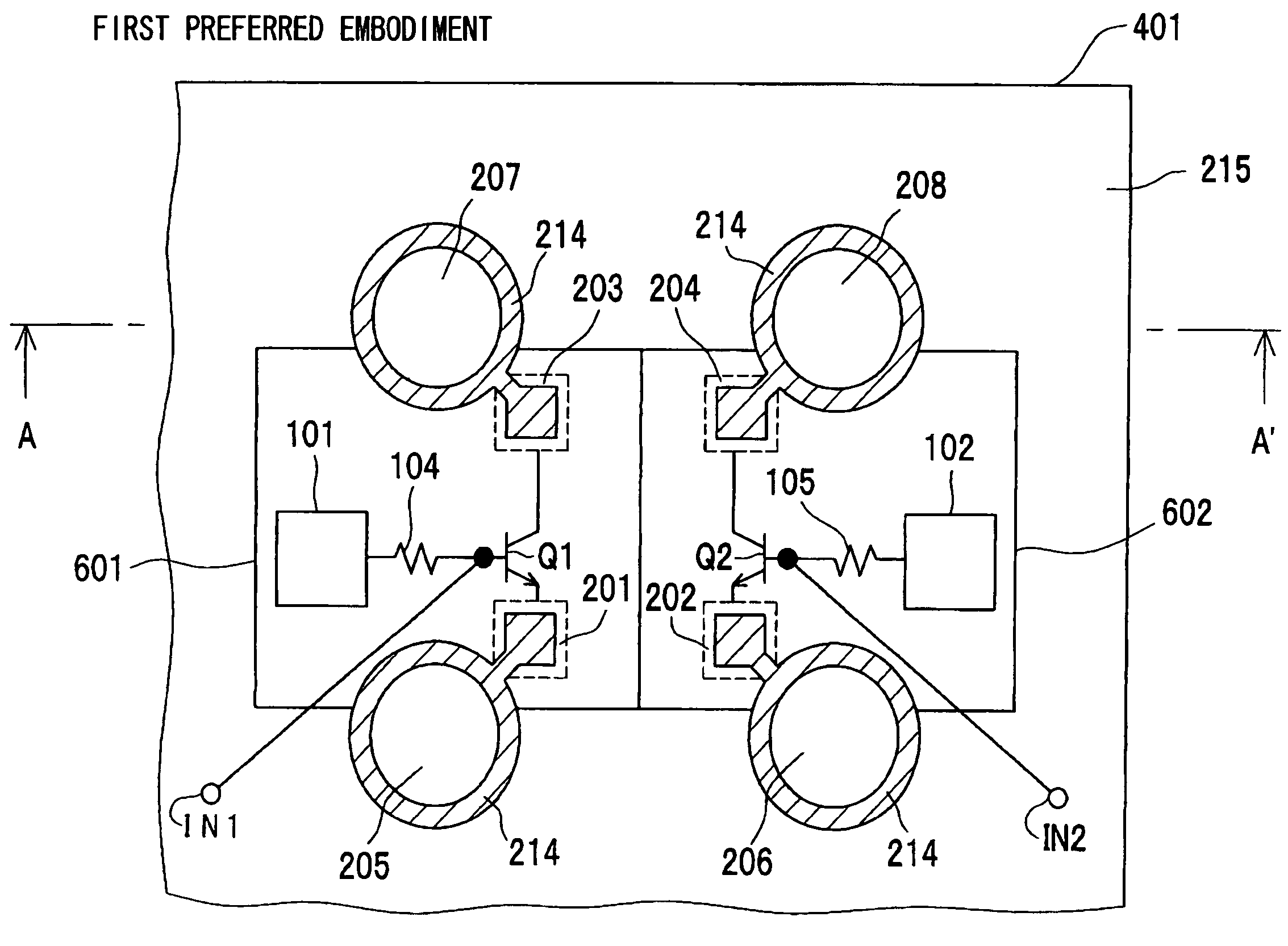
[0032]FIG. 1 is a schematic plan view showing a configuration of high-frequency differential amplifier circuitry according to a first preferred embodiment of the present invention. FIG. 1 shows a state in which a resin 213 (See FIG. 2) is not formed on a semiconductor substrate 401. The high-frequency differential amplifier circuitry according to the first preferred embodiment is formed on the semiconductor substrate 401 having a chip size package, which forms a rewiring layer on the chip. Referring to FIG. 1, the high-frequency differential amplifier circuitry is configured by including transistors Q1 and Q2, bias circuits 101 and 102, resistors 104 and 105, pads 201, 202, 203 and 204, CSP (chip size package) output terminals 205, 206, 207 and 208, and input terminals IN1 and IN2. The transistors Q1 and Q2 constitute a differential pair. Bases of the transistors Q1 and Q2 are connected with the resistors 104 and 105, respectively, collectors thereof are connected with the pads 203 ...

second preferred embodiment

[0039]FIG. 6 is a schematic plan view showing a configuration of a high-frequency differential amplifier circuitry according to a second preferred embodiment of the present invention. As shown in FIG. 6, the high-frequency differential amplifier circuitry according to the second preferred embodiment is different from that of the first preferred embodiment shown in FIG. 1 in that the CSP output terminals 205 and 206 are connected with each other via the rewiring layer 214. The other aspects are similar to those of the high-frequency differential amplifier circuitry according to the first preferred embodiment of FIG. 1, and detailed descriptions of the components that are denoted by the same reference numerals as those of FIG. 1 are omitted.

[0040]FIG. 7 is a cross-sectional view taken along line B-B′ of FIG. 6. Referring to FIG. 7, the CSP output terminals 205 and 206 are connected with each other via the copper post 212, which is formed beneath the respective CSP output terminals 205...

third preferred embodiment

[0042]FIG. 8 is a schematic plan view showing a configuration of high-frequency differential amplifier circuitry according to a third preferred embodiment of the present invention. As shown in FIG. 8, the high-frequency differential amplifier circuitry according to the third preferred embodiment is different from that of the second preferred embodiment shown in FIG. 6 in that the subcontact 301 is formed about the circumference of and between the cells 601 and 602, and that a pad 209 and a CSP output terminal 210 are additionally formed. The other aspects are similar to those of the high-frequency differential amplifier circuitry of the second preferred embodiment of FIG. 6, and detailed descriptions of components that are denoted by the same reference numerals as those of FIG. 6 are omitted.

[0043]Referring to FIG. 8, the subcontact 301 is a grounding conductor, surrounds the cell 601 and the cell 602, and is connected with the pad 209. The CSP output terminal 210 is connected with ...


PUM


Abstract

In differential amplifier circuitry formed on a semiconductor substrate, first and second transistors constitute a differential pair of the differential amplifier circuitry. First and second pads are connected with emitters of the first and second transistors, respectively. The first and second pads are connected with first and second external ground terminals via first and second rewiring layers to be grounded, respectively. The first and second rewiring layers are preferably connected with each other. Further, bases of the first and second transistors are connected with first and second bias circuits via first and second resistors, respectively.

Description

BACKGROUND OF THE INVENTION[0001]1. Field of the Invention[0002]The present invention relates to differential amplifier circuitry formed on a semiconductor substrate. In particular, the present invention relates to differential amplifier circuitry formed on a semiconductor substrate with a rewiring technique.[0003]2. Description of the Prior Art[0004]FIG. 12 shows a circuit diagram of high-frequency differential amplifier circuitry according to a prior art (See Japanese Patent Laid-Open Publication No. JP-2003-133862-A). Referring to FIG. 12, the high-frequency differential amplifier circuitry is configured by transistors Q1 and Q2, a bias circuit 103, resistors 104 and 105, pads 201, 203 and 204, CSP (Chip Size Package) output terminals 205, 207 and 208, and input terminals IN1 and IN2. The transistors Q1 and Q2 constitute a differential pair of the differential amplifier circuit. The bias circuit 103 generates a predetermined bias current, and supplies the bias current to a base o...

Claims


Application Information

Patent Timeline
Patent Type & Authority Patents(United States)
IPC IPC(8): H03F3/45
CPCH01L27/016H03F3/45085H03F2200/372H03F2203/45464H03F2203/45594H01L2224/11H01L2224/05569H01L2224/05008H01L2224/05022H01L2224/05001H01L2224/05124H01L2224/05647H01L2224/06131H01L24/05H01L2924/00014
Inventor NAKAMURA, MASANORIKOJIMA, IWAO
Owner PANASONIC CORP
Why Eureka
Try Eureka