Static RAM having a TFT with n-type source and drain regions and a p-type region in contact with only the intrinsic channel of the same

a static ram and source and drain technology, applied in non-linear optics, instruments, optics, etc., can solve the problems of not being able to reduce the size of the tft formed, driving up the cost of production, and high cost of quartz glass, so as to improve the display quality, and simplify the circuitry

Inactive Publication Date: 2006-02-21
PANASONIC LIQUID CRYSTAL DISPLAY CO LTD +1
View PDF9 Cites 0 Cited by
  • Summary
  • Abstract
  • Description
  • Claims
  • Application Information

AI Technical Summary

Benefits of technology

[0012]The object of the present invention is to provide a TFT of a structure of which the characteristics are not deteriorated in the gate-negative pulse mode.
[0013]Moreover, the object of the present invention is to provide a liquid crystal display device which features a simplified circuitry and improved display quality by employing a TFT which is less deteriorated in the gate-negative pulse mode, for a liquid crystal display device of which the circuitry is becoming complex or of which the display quality is becoming poor due to limitation on the range when utilizing the TFT which is deteriorated in the gate-negative pulse mode.
[0014]Furthermore, it is the object of the present invention to provide a liquid crystal display device equipped with a shift register having improved reliability by employing a TFT which is less deteriorated in the gate-negative pulse mode, for the shift register.
[0015]Moreover, it is the object of the present invention to provide a liquid crystal display device using an analog switch having improved reliability by utilizing a TFT which is less deteriorate in the gate-negative pulse mode, for the analog switch.
[0016]According to the present invention, the above-mentioned objects are accomplished by providing a semiconductor thin film of the TFT with a p-type semiconductor region that is in contact with a channel region but is electrically connected to nowhere except the channel region. Upon employing this structure, holes induced on the surface by the gate-negative pulses are further supplied from the p-type semiconductor region. The holes supplied from the p-type semiconductor region relax the electric field established by the gate-negative pulse. Therefore, the hot holes are less injected into the gate oxide film, and the TFT characteristics are less deteriorated. Besides, the p-type semiconductor region needs be connected to nowhere except the channel region and can, hence, be replaced by the conventional TFT, and an increase in the TFT area is confined to the p-type semiconductor region only.

Problems solved by technology

However, it was not allowed to decrease the size of the TFT formed by amorphous silicon since its current driving ability was so small.
However, quartz glass is very expensive and drives up the cost of production.
The hot carrier that is injected into the gate oxide film causes a problem of deterioration in the characteristics of TFT.

Method used


Image

  • Static RAM having a TFT with n-type source and drain regions and a p-type region in contact with only the intrinsic channel of the same
  • Static RAM having a TFT with n-type source and drain regions and a p-type region in contact with only the intrinsic channel of the same
  • Static RAM having a TFT with n-type source and drain regions and a p-type region in contact with only the intrinsic channel of the same

Examples


embodiment 1

[Embodiment 1]

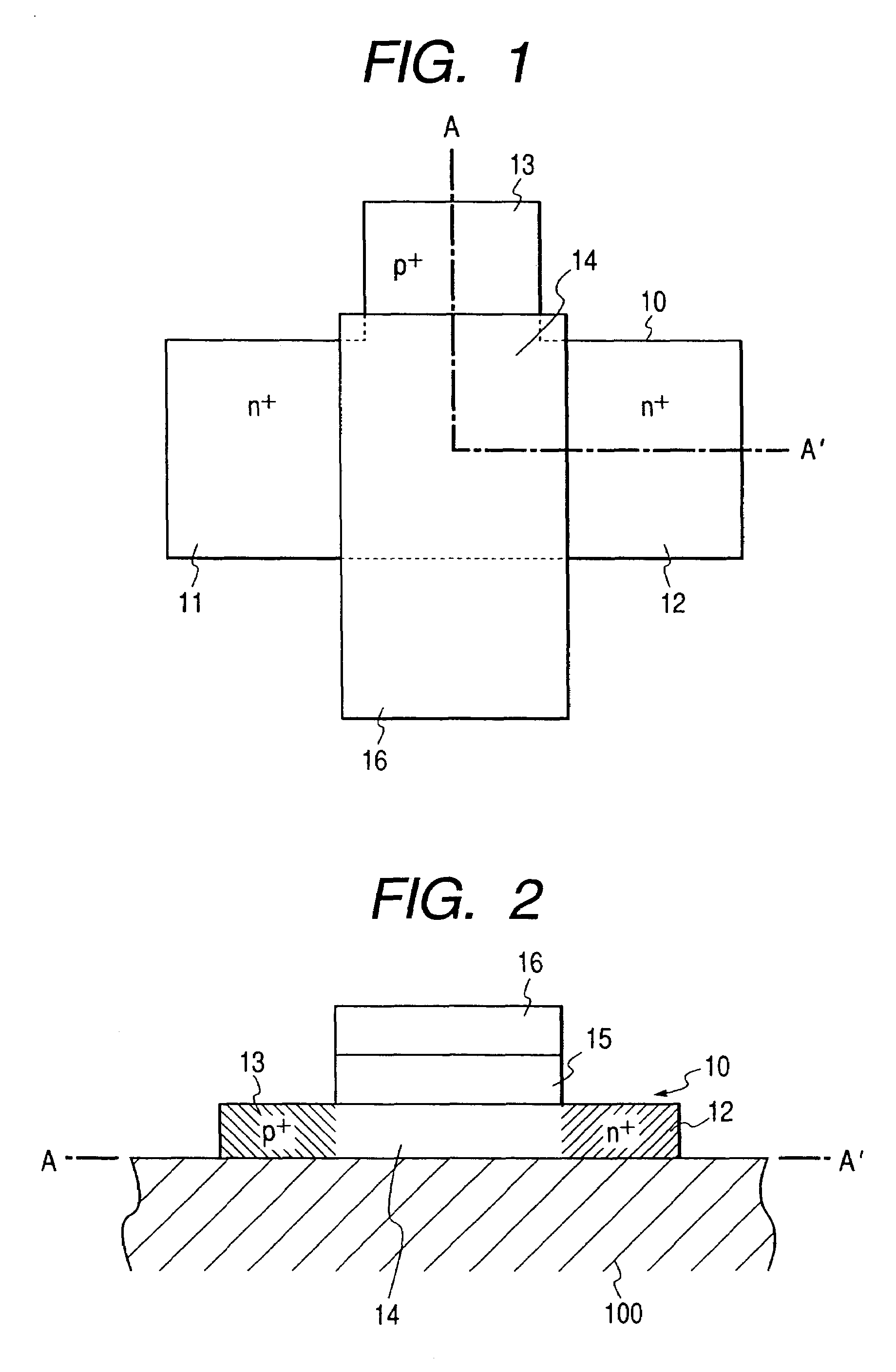
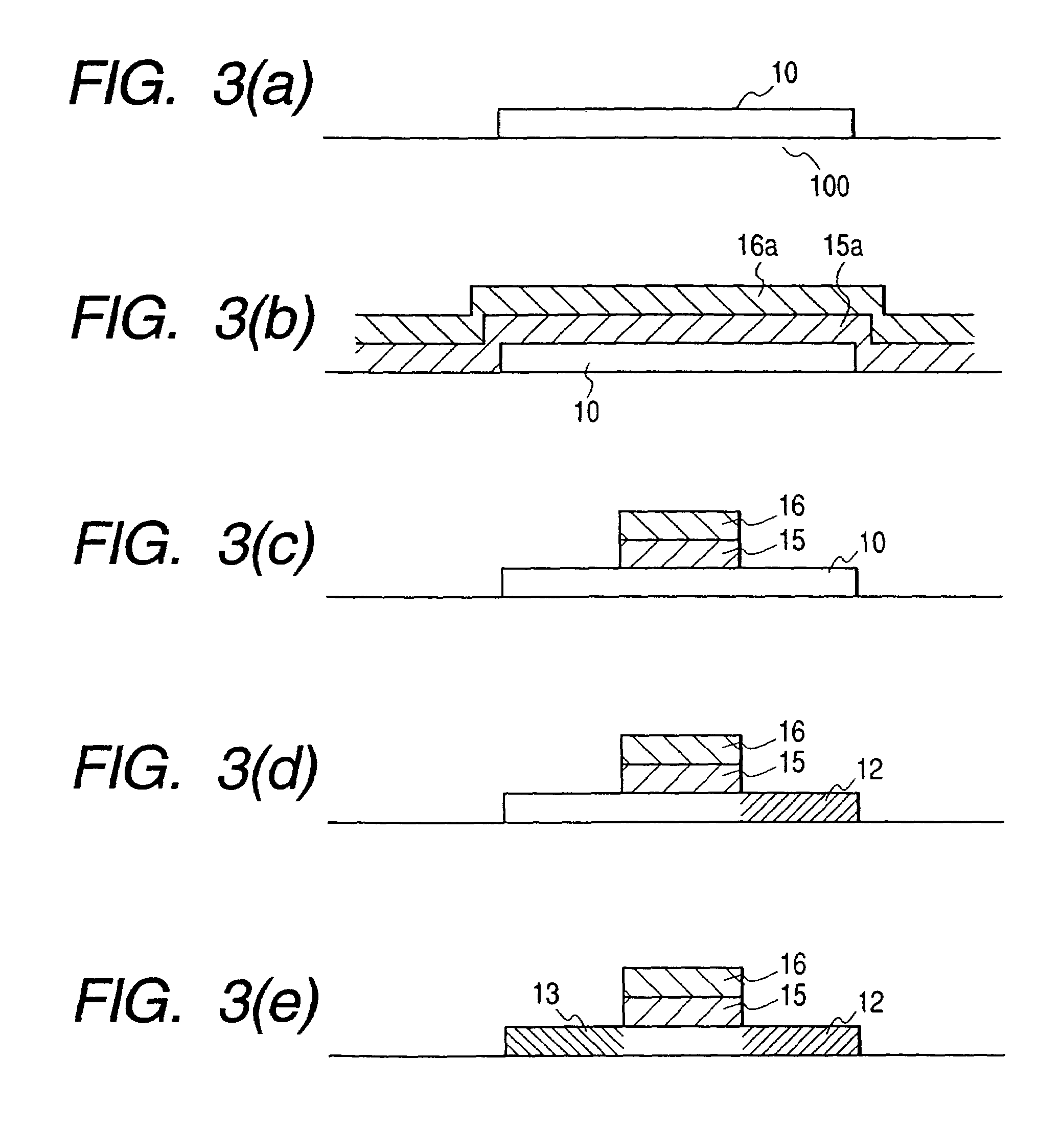
[0043]FIG. 1 is a schematic plan view illustrating a TFT according to the present invention, and FIG. 2 is a schematic sectional view along a line A–A′ in FIG. 1. A substrate is a glass 100. A first layer is a thin polysilicon film 10. The thin polysilicon film 10 is constituted by a source 11 and a drain 12 which are n-type semiconductor regions, a p-type semiconductor region 13, and a channel region 14 just under a gate 16 which is an intrinsic semiconductor region. A second layer is a gate insulating film 15 which insulates the gate 16 and the thin polysilicon film 10 from each other. A third layer is the gate 16 having the same shape as the gate insulating film 15. Upon applying a positive voltage to the gate 16, an inverted layer in which the electrons are present in an excess amount is formed in the channel region 14 to form a channel, whereby the source 11 and the drain 12 are rendered conductive to each other to obtain a switching operation.

[0044]In the TFT str...

embodiment 2

[Embodiment 2]

[0048]FIG. 5 is a schematic plan view of a bottom gate type TFT according to the present invention, and FIG. 6 is a schematic sectional view along a line A–A′ in FIG. 5. A substrate is a glass 100. A first layer is a gate 16. A second layer is a gate insulating film 15 which insulates the gate 16 and a thin polysilicon film 10 from each other. A third layer is the thin polysilicon film 10. In the thin polysilicon film 10 are formed a source 11 and a drain 12 which are n-type semiconductor regions, a p-type semiconductor region 13, and a channel region 14 which is an intrinsic semiconductor region just over the gate electrode. A fourth layer is a channel protection film 50 for protecting the channel. Upon applying a positive voltage to the gate 16, an inverted layer in which the electrons are present in an excess amount is formed in the channel region 14 thereby to form a channel, whereby the source 11 and the drain 12 are rendered conductive relative to each other to o...

embodiment 3

[Embodiment 3]

[0049]FIG. 7 is a schematic sectional view of an SOI-MOSFET according to the present invention. FIG. 7 corresponds to FIG. 2 and FIG. 6, and in which are appearing a drain 12 and a p-type semiconductor region 13 in a semiconductor film 17. An insulating layer 19 is formed on a semiconductor substrate 18, and the semiconductor film 17 which is the first layer is formed on the insulating layer 19. The semiconductor film 17 is formed by, for example, single crystalline silicon or a single crystal of gallium-arsenic. The semiconductor film 17 is constituted by a source and a drain 12 which are n-type semiconductor regions, a p-type semiconductor region 13, and a channel region 14 which is an intrinsic semiconductor region just under the gate. A second layer is a gate insulating film 15 which insulates the gate 16 and the semiconductor film 10 from each other. A third layer is the gate 16 having the same shape as the gate insulating film 15. Upon applying a positive voltage...


PUM

PropertyMeasurementUnit
temperatureaaaaaaaaaa
thicknessaaaaaaaaaa
semiconductoraaaaaaaaaa

Abstract

To prevent an n-channel thin-film transistor from being deteriorated by hot holes generated in a gate-negative pulse mode. A thin polysilicon film 10 is provided with a p-type semiconductor region 13 in contact with a channel region 14. The p-type semiconductor region 13 is electrically connected to nowhere except the channel region 14. Holes induced on the surface due to a gate-negative pulse are further supplied from the p-type semiconductor region 13. An electric field established by the gate-negative pulse is relaxed by the holes, fewer hot holes are injected into the gate oxide film, and the TFT characteristics are less deteriorated.

Description

CROSS-REFERENCE TO RELATED APPLICATIONS[0001]This application is a Continuation application of application Ser. No. 09 / 694,486, filed Oct. 24, 2000 now U.S. Pat. No. 6,611,300 which was a Continuation application of application Ser. No. 09 / 074,314, filed May 8, 1998, now U.S. Pat. No. 6,166,786, the entire disclosure of which is hereby incorporated by reference.BACKGROUND OF THE INVENTION[0002]The present invention relates to a liquid crystal display device of an active matrix type used for displaying image data and character data from OA equipment or the like, and to the structure of an n-channel thin-film transistor used for this device.[0003]A thin-film transistor (hereinafter abbreviated as TFT) has heretofore been used for driving liquid crystals of a pixel in a panel of a liquid crystal display device of the directly-viewing type. A simple switching element suffices for the performance of the TFT and, hence, amorphous silicon has been used as a semiconductor thin film. On the ...

Claims


Application Information

Patent Timeline
Patent Type & Authority Patents(United States)
IPC IPC(8): H01L27/01G02F1/136G02F1/1368H01L21/336H01L27/12H01L29/786
CPCG02F1/1368H01L29/78615H01L29/66757H01L27/12H01L27/1214H01L29/78696
Inventor OHKUBO, TATSUYAKAWACHI, GENSHIROMIKAMI, YOSHIROMASUDA, KAZUHITOKAGEYAMA, HIROSHI
Owner PANASONIC LIQUID CRYSTAL DISPLAY CO LTD
Why Eureka
Try Eureka