Transistors having controlled conductive spacers, uses of such transistors and methods of making such transistors

a technology of conductive spacers and transistors, applied in the field of transistor structures, can solve the problems of disadvantages of ldd transistors in their own way, and achieve the effect of improving the drive current of transistors and reducing delays in integrated circuits

Inactive Publication Date: 2006-02-28
MICRON TECH INC
View PDF18 Cites 41 Cited by
  • Summary
  • Abstract
  • Description
  • Claims
  • Application Information

AI Technical Summary

Benefits of technology

[0008]Thus, the present invention provides an improved transistor structure which includes an insulated electrically conductive gate spacer or electrically conductive gate spacer portion which is contacted and controlled separately from the gate of the transistor. The improved transistor structure also provides improved transistor drive current and reduced delays within integrated circuits including the improved transistors. The improved transistor structure can be used together with LDD transistors and other conventional transistors at least, for example, in critical speed paths. The present invention also provides uses for the improved transistor structure and methods for making it, and uses for the combined LDD / conventional and improved transistor structures and methods for making the combined LDD / conventional and improved transistor structures.

Problems solved by technology

While LDD transistors are an improvement over conventional MOS transistors, LDD transistors also have disadvantages in their own right.

Method used


Image

  • Transistors having controlled conductive spacers, uses of such transistors and methods of making such transistors
  • Transistors having controlled conductive spacers, uses of such transistors and methods of making such transistors
  • Transistors having controlled conductive spacers, uses of such transistors and methods of making such transistors

Examples


first embodiment

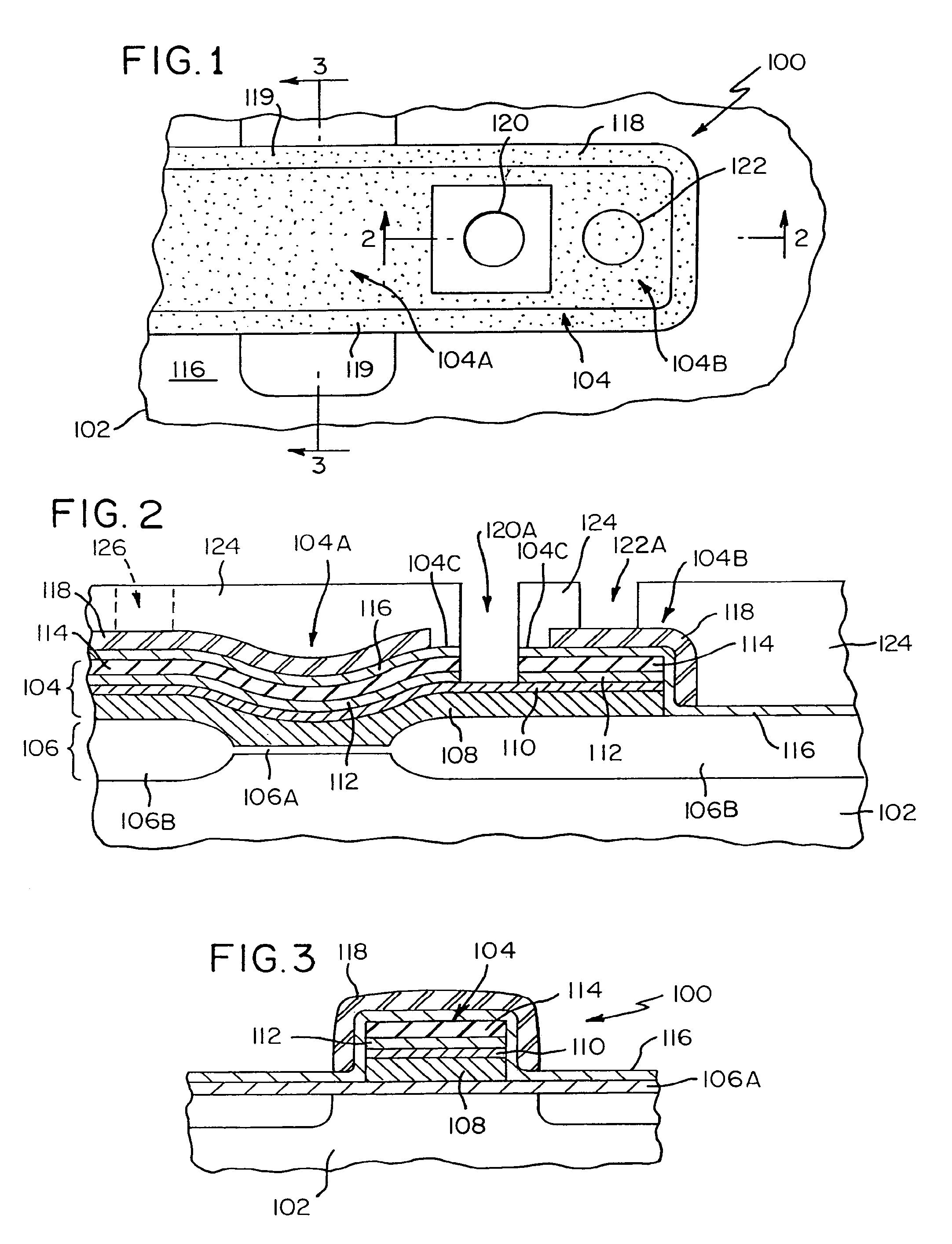
[0022]An improved transistor 100 or multiple gate transistor including the structure of a first embodiment and made in accordance with the invention of the present application is shown in FIGS. 1–3. The transistor 100 is formed on a base layer or semiconductor structure 102 which can be one or more semiconductor layers or structures and includes active or operable portions of semiconductor devices. The semiconductor structure 102 is formed of silicon in the illustrated embodiment although the invention is applicable to other semiconductor materials. A gate structure 104 is formed on a first oxide layer 106 formed on the semiconductor structure 102. The gate structure 104 is illustrated as a multilayer gate stack which may be formed for an array device for which the present invention is initially being used. However, other gate structures can be used and are considered to be within the scope of the present invention.

[0023]The first oxide layer 106 includes thin gate oxide regions rep...

second embodiment

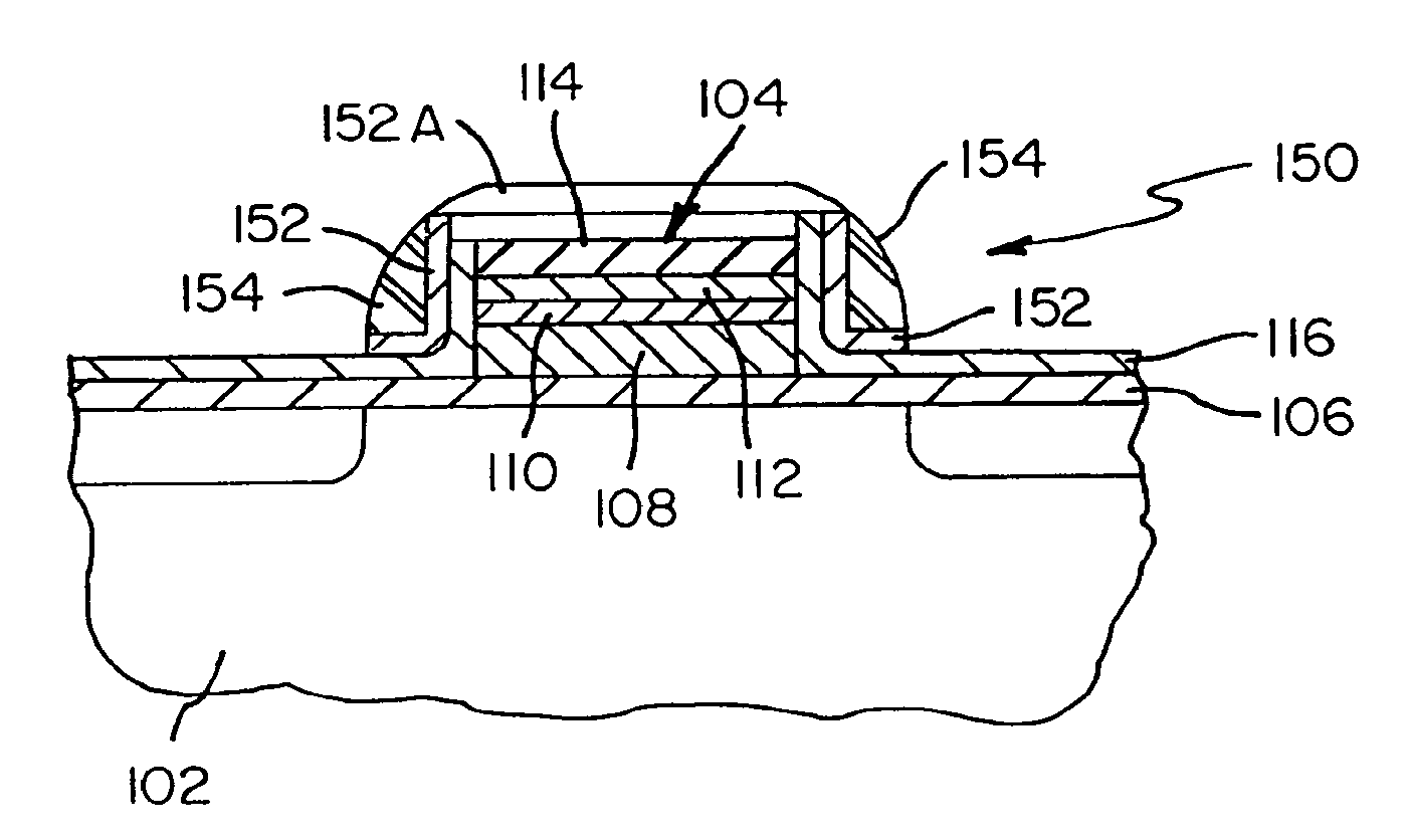
[0035]An improved transistor 150 including the structure of a second embodiment and made in accordance with the invention of the present application is shown in FIGS. 7 and 8. Structure which is common between the transistor of FIGS. 1–3 and FIGS. 7 and 8 will be labeled with like numbers. The transistor 150 is formed on a base layer or semiconductor structure 102 which can be one or more semiconductor layers or structures and includes active or operable portions of semiconductor devices. The semiconductor structure 102 is formed of silicon in the illustrated embodiment although the invention is applicable to other semiconductor materials. A gate structure 104 is formed on a first oxide layer 106 formed on the semiconductor structure 102. The gate structure 104 is illustrated as a multilayer gate stack which may be formed for an array device for which the present invention is initially being used. However, other gate structures can be used and are considered to be within the scope o...

third embodiment

[0038]a multiple gate transistor of the present invention is illustrated in FIGS. 9 and 10. In particular, a three gate transistor 160 is formed on a base layer or semiconductor structure 162 which can be one or more semiconductor layers or structures and includes active or operable portions of semiconductor devices. The semiconductor structure 162 is formed of silicon in the illustrated embodiment although the invention is applicable to other semiconductor materials. A gate structure 164 is formed on a first oxide layer 166 formed on the semiconductor structure 162. The gate structure 164 is illustrated as a polysilicon gate; however, other gate structures can be used and are considered to be within the scope of the present invention.

[0039]A secondary oxide layer 168 is formed on the gate structure 164. The secondary oxide layer 168 may be formed, for example, by a chemical vapor deposition (CVD) of tetraethyl orthosilicate (TEOS) or rapid thermal processor (RTP) oxide (RTO). A con...


PUM


Abstract

A transistor structure includes an insulated conductive gate spacer or a conductive layer under a nonconductive spacer, together forming a composite spacer, which is contacted and driven separately from the conventional gate of the transistor. The gate spacer, conductive layer of a composite spacer or a portion or portions thereof serve as a control or controls for the transistors taking the form of a second gate or second and third gates for the transistors. The transistors may be used throughout an integrated circuit or it may be preferred to use the improved transistor only in critical speed paths of an integrated circuit. Delays within circuits including the improved transistors are reduced since the drain voltage can be higher than VCC and the BVDSS and subthreshold voltage are substantially higher than standard LDD transistors. When the improved transistors are used selectively within an integrated circuit, the remaining devices can be structured as standard LDD transistors, using the gate spacers in a conventional manner, and/or as conventional transistors.

Description

CROSS-REFERENCE TO RELATED APPLICATIONS[0001]This application is a continuation of U.S. patent application Ser. No. 08 / 987,819, filed Dec. 10, 1997 now U.S. Pat. No. 6,005,273 and entitled TRANSISTORS HAVING CONTROLLED CONDUCTIVE SPACERS, USES OF SUCH TRANSISTORS AND METHODS OF MAKING SUCH TRANSISTORS the disclosure of which is hereby incorporated by reference which is a continuation-in-part of U.S. patent application Ser. No. 08 / 741,828, filed Oct. 31, 1996 now U.S. Pat. No. 5,714,786 and entitled TRANSISTORS HAVING CONTROLLED CONDUCTIVE SPACERS, USES OF SUCH SPACERS AND METHODS OF MAKING SUCH TRANSISTORS the disclosure of which is hereby incorporated by reference.BACKGROUND OF THE INVENTION[0002]The present invention relates in general to transistor structures and, more particularly, to improved transistor structures, their uses and methods for making them wherein an insulated conductive gate spacer or an insulated conductive portion of a gate spacer is contacted and driven separa...

Claims


Application Information

Patent Timeline
Patent Type & Authority Patents(United States)
IPC IPC(8): H01L29/78H01L27/108H01L21/28H01L21/336H01L21/8234H01L27/088H01L29/49
CPCH01L21/28132H01L21/823468H01L29/7831H01L29/4983H01L29/66484H01L27/088H01L21/28114H10B12/00
Inventor GONZALEZ, FERNANDOKAO, DAVID
Owner MICRON TECH INC
Why Eureka
Try Eureka