Ultraviolet detector and manufacture method thereof

Inactive Publication Date: 2006-03-07
NAT CENT UNIV
View PDF2 Cites 23 Cited by
  • Summary
  • Abstract
  • Description
  • Claims
  • Application Information

AI Technical Summary

Benefits of technology

[0005]As mentioned above, a conventional P-type or N-type semiconductor layer in a photoelectric element for light detection is generally a multi-layer structure vegetated by multi-layer epitaxial technology, therefore, an incident light is

Problems solved by technology

Another weakness of the multi-layer epitaxial technology is

Method used


Image

  • Ultraviolet detector and manufacture method thereof
  • Ultraviolet detector and manufacture method thereof
  • Ultraviolet detector and manufacture method thereof

Examples


Embodiment Construction

[0018]At least a preferred embodiment is described below with reference to the annexed drawings, in which partial measurements are exaggeratedly expressed for easy viewing.

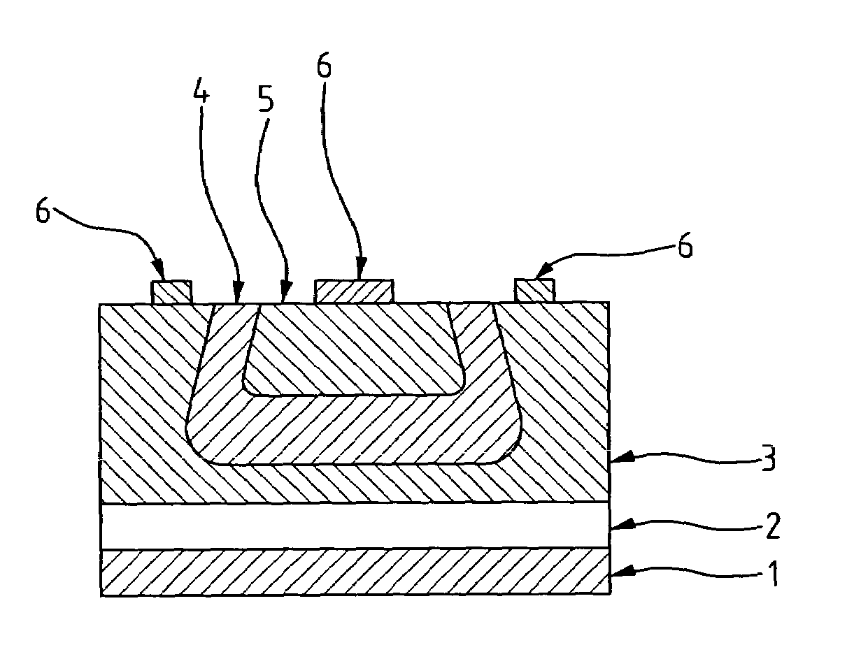
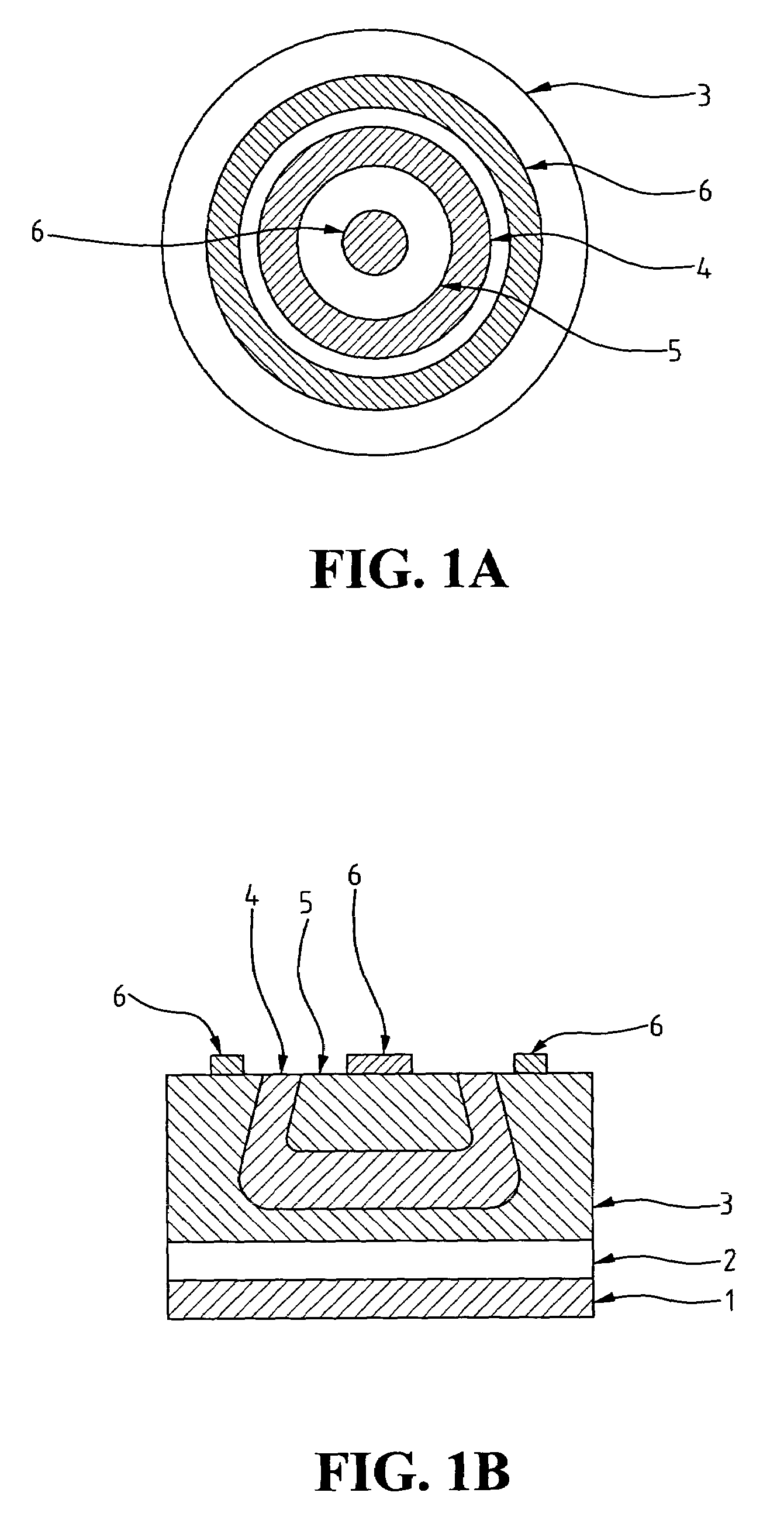
[0019]As illustrated in an embodiment of an ultraviolet detector of the present invention shown in FIGS. 1A and 1B, the detector is comprised of a baseplate 1, a buffer layer 2, and a P-type GaN layer 3. Enclosed by the P-type GaN layer 3, a first N-type GaN layer 4 is extended to the top end of the P-type GaN layer 3, and in turn, a second N-type GaN layer 5 enclosed by the first N-type GaN layer 4 is also extended to the top end. Moreover, untouched to and outside of the first N-type GaN layer 4, an annular metallic layer 6 is formed on the top end of the P-type GaN layer 3. Also, another metallic layer 6 is formed on the top end within the scope inside the second N-type GaN layer 5.

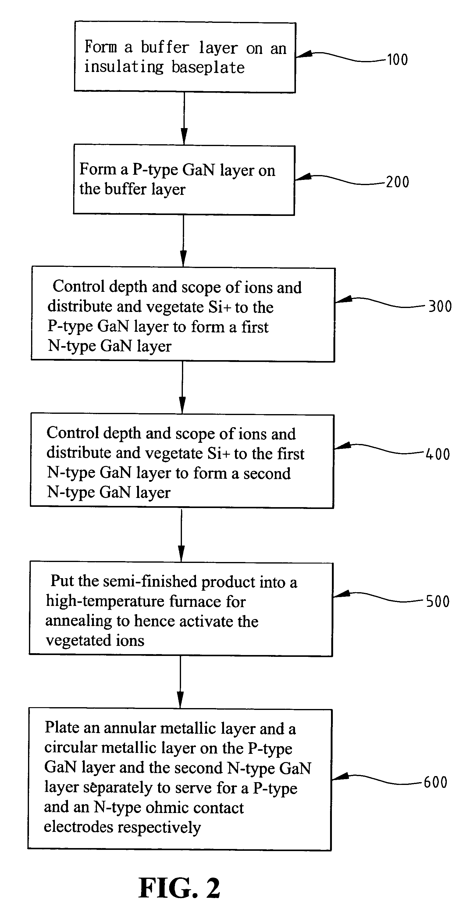
[0020]Also referring to FIG. 2, the manufacture process of the ultraviolet detector of the present invention comprises the followin...


PUM


Abstract

The present invention relates to an ultraviolet detector and manufacture method thereof, in which a buffer layer is formed on a baseplate and a P-type GaN layer is formed on the baseplate by using epitaxial method. By availing ion-distribution-and-vegetation technology, a first N-type GaN layer is vegetated and invested in the P-type GaN layer by distributing and vegetating Si+ ions in that layer, and a second N-type GaN layer having a thicker ion concentration is invested in the N-type GaN layer. Finally, an annular and a circular metallic layer are formed between the P-type GaN layer and the first N-type GaN layer as well as inside the second N-type GaN layer, respectively, to serve for respective ohmic contact layers. The present invention is characterized in that an incident light can project upon a depletion layer of the GaN planar structure to have the detection efficiency significantly improved.

Description

BACKGROUND OF THE INVENTION[0001]1. Field of the Invention[0002]The present invention relates generally to an ultraviolet detector and manufacture method thereof, and more particularly to that capable of improving photon efficiency and simplifying manufacture process to raise yield, lower down cost, and promote the function of photoelectric elements through an ion-distribution technology by vegetating an N-type GaN (Gallium nitride) layer in a P-type GaN layer and creating a planar structure containing P-type and N-type GaN layers on the top face of the element to enable an incident light, such as an ultraviolet beam, to enter a depletion layer directly for easy detection.[0003]2. The Prior Arts[0004]An incident light is applied to penetrate through a P-type and an N-type semiconductor layer when a photoelectric element for photo-detection is in operation. In the case the photon energy of a incident light is larger than a band gap of the semiconductor material, the photon energy wil...

Claims


Application Information

Patent Timeline
IPC IPC(8): G01J1/42H01L31/0352H01L31/103H01L31/18
CPCG01J1/429H01L31/03529H01L31/184H01L31/1035Y02E10/544Y02P70/50
Inventor CHI, GOU-CHUNGSHEU, IINN-KONGCHEN, MENG-CHELEE, MIN-LUM
Owner NAT CENT UNIV
Why Eureka
Try Eureka