Semiconductor light emitting device and method of fabricating the same

a technology of semiconductors and light emitting devices, which is applied in the direction of semiconductor laser arrangements, optical resonator shape and construction, and semiconductor lasers. it can solve the problems of difficult fusion bonding of entire substrate surfaces and unstable light emitting wavelength, and achieve the effect of low threshold curren

Inactive Publication Date: 2006-03-07
PANASONIC CORP
View PDF13 Cites 23 Cited by
  • Summary
  • Abstract
  • Description
  • Claims
  • Application Information

AI Technical Summary

Benefits of technology

[0013]The present invention has been developed under the circumstances, and an object of the present invention is to provide a semiconductor light emitting device with a low threshold current and with polarization planes of light controlled, and a method of fabricating the semiconductor light emitting device.

Problems solved by technology

Even in the light having the same polarization plane, the light emitting wavelength becomes unstable because of the presence of two stable light emitting modes.
Although the semiconductor light emitting device is fabricated by fusion bonding crystals to each other as described above, the entire surfaces of the substrates having a large diameter are difficult to fusion bond.

Method used


Image

  • Semiconductor light emitting device and method of fabricating the same
  • Semiconductor light emitting device and method of fabricating the same
  • Semiconductor light emitting device and method of fabricating the same

Examples


embodiment 2

(Embodiment 2)

[0084]In a second embodiment, a description will be given of a semiconductor light emitting device configured to have photonic crystal as in the first embodiment and have a period of the photonic crystal in the resonator direction and a period of the photonic crystal in the direction perpendicular to the resonator direction which differ from each other.

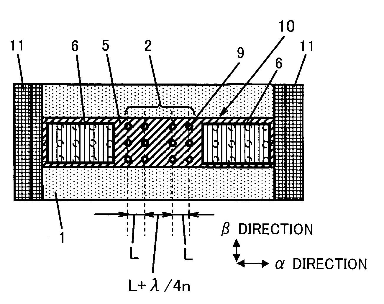
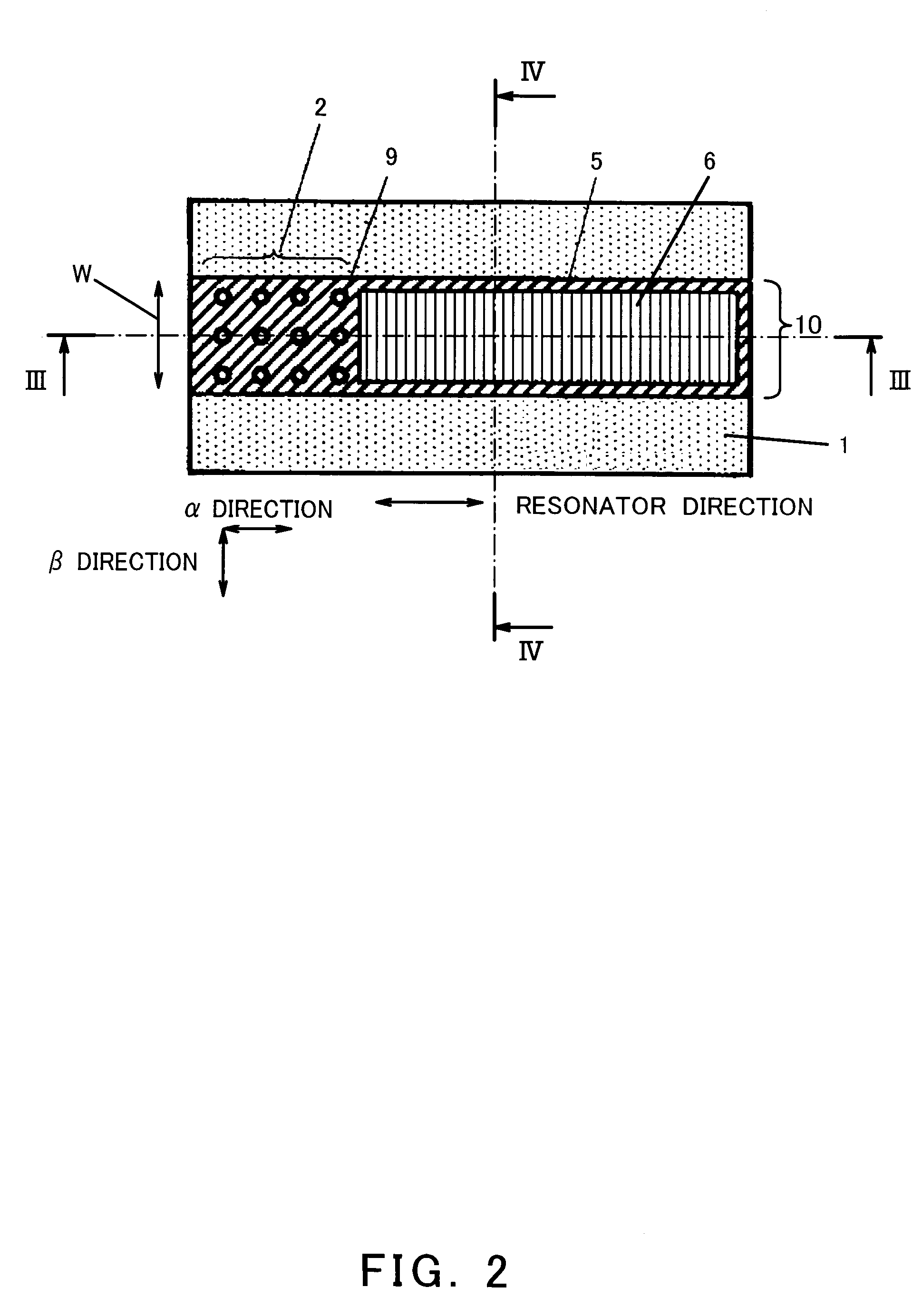
[0085]FIG. 8 is a plan view showing a structure of a semiconductor light emitting device according to the second embodiment of the present invention. As shown in FIG. 8, the photonic crystal structure 2 is formed by arranging a plurality of concave portions 9 in the shape of rectangular lattice. Here, a period of the concave portions 9 in the resonator direction (spacing between adjacent concave portions 9) F1 is longer than a period F2 of the concave portions 9 in the direction perpendicular to the resonator direction. In FIG. 8, reference numeral 13 denotes a growth region where the p-type InP upper cladding layer is s...

embodiment 3

(Embodiment 3)

[0101]In a third embodiment, there is illustrated a semiconductor light emitting device capable of avoiding leakage of spontaneous emission light and stimulated emission light in the resonator direction by forming reflection films on end faces of a stripe structure to reflect light.

[0102]FIGS. 11A and 11B are views showing a structure of the semiconductor light emitting device according to the third embodiment of the present invention, in which FIG. 11A is a plan view and FIG. 11B is a view taken in the direction of arrows along line A—A in FIG. 11A. As shown in FIGS. 11A and 11B, insulator multi-layered thin films 11 comprising alumina and titania are provided on both end faces of the stripe structure 10. Since the other structure of the semiconductor light emitting device of this embodiment is identical to that of the first embodiment, the same or corresponding parts are identified by the same reference numerals and will not be further described.

[0103]Subsequently, a...

embodiment 4

(Embodiment 4)

[0109]In a fourth embodiment, there is shown a semiconductor light emitting device capable of inhibiting a mode from becoming unstable due to fluctuation of a phase of light on a reflection plane by forming a photonic crystal structure over the entire stripe structure.

[0110]FIGS. 13A and 13B are views showing a structure of the semiconductor light emitting device according to the fourth embodiment of the present invention, in which FIG. 13A is a plan view and FIG. 13B is a view taken in the direction of arrows along line C—C in FIG. 13A.

[0111]As shown in FIGS. 13A and 13B, cylindrical concave portions 9 are formed in the shape of rectangular lattice over the entire p-type InP upper cladding layer 5 in stripe shape. Since the other structure of the semiconductor light emitting device of this embodiment is identical to that of the third embodiment, the same or corresponding parts are identified by the same reference numerals and will not be further described.

[0112]Subseq...


PUM


Abstract

A semiconductor light emitting device of the present invention comprises a n-type InP substrate (1), and a stripe structure (10) formed in the stripe shape on the n-type InP substrate (1) and comprised of a n-type InP lower cladding layer (3), an active layer (4) having a resonator in a direction parallel to the n-type InP substrate (1), and a p-type InP upper cladding layer (5). The stripe structure (10) has a photonic crystal structure (2) with concave portions 9 arranged in rectangular lattice shape, and the direction in which the concave portions (9) of the photonic crystal structure (2) are arranged corresponds with a resonator direction. A stripe-shaped upper electrode (6) is formed on the stripe structure (10) to extend in the resonator direction. The semiconductor light emitting device of the present invention so structured is configured to radiate light in the direction perpendicular to the n-type InP substrate (1).

Description

[0001]This is a continuation application under 35 U.S.C.111(a) of pending prior International Application No. PCT / JP03 / 01285, filed on Feb. 7, 2003.BACKGROUND OF THE INVENTION[0002]1. Field of the Invention[0003]The present relates to a semiconductor light emitting device of a surface emitting type using photonic crystal grown on a substrate and a method of fabricating the same.[0004]2. Description of the Related Art[0005]The conventional semiconductor light emitting devices using photonic crystal are disclosed in, for example, Japanese Laid-Open Patent Application Publication No. Hei. 11-330619, Japanese Laid-Open Patent Application Publication No. 2001-308457, Japanese Laid-Open Patent Application Publication No. 2001-9800 (U.S. patent Publication No. 2002 / 0109134 specification), Japanese Laid-Open Patent Application Publication No. Sho 63-205984 (U.S. Pat. No. 4,847,844 specification), and Japanese Laid-Open Patent Application Publication No. 2002-062554.[0006]Likewise, the semic...

Claims


Application Information

Patent Timeline
Patent Type & Authority Patents(United States)
IPC IPC(8): H01L33/00H01S5/028H01S5/10H01S5/12H01S5/18H01S5/187H01S5/22H01S5/40H01S5/42
CPCH01S5/42H01S5/187H01S5/028H01S5/105H01S5/2201H01S5/124H01S5/11
Inventor OTSUKA, NOBUYUKIYOSHII, SHIGEOYOKOGAWA, TOSHIYA
Owner PANASONIC CORP
Why Eureka
Try Eureka