Display apparatus and display method

Inactive Publication Date: 2006-03-07
SHARP KK
View PDF25 Cites 30 Cited by
  • Summary
  • Abstract
  • Description
  • Claims
  • Application Information

AI Technical Summary

Benefits of technology

[0010]The objective of the present invention is to provide a display apparatus which can effectively detect current

Problems solved by technology

However, it is difficult to construct the constant current source in reality and hence a constant current drive circuit is arranged using a constant voltage source.
Thus the measurement of the current of each organic EL device 124 can be carried out only on a device-by-device basis so that it is not possible to ef

Method used


Image

  • Display apparatus and display method
  • Display apparatus and display method
  • Display apparatus and display method

Examples


first embodiment

[0073]Referring to FIGS. 1 to 4, a first embodiment in accordance with the present invention will be described as below.

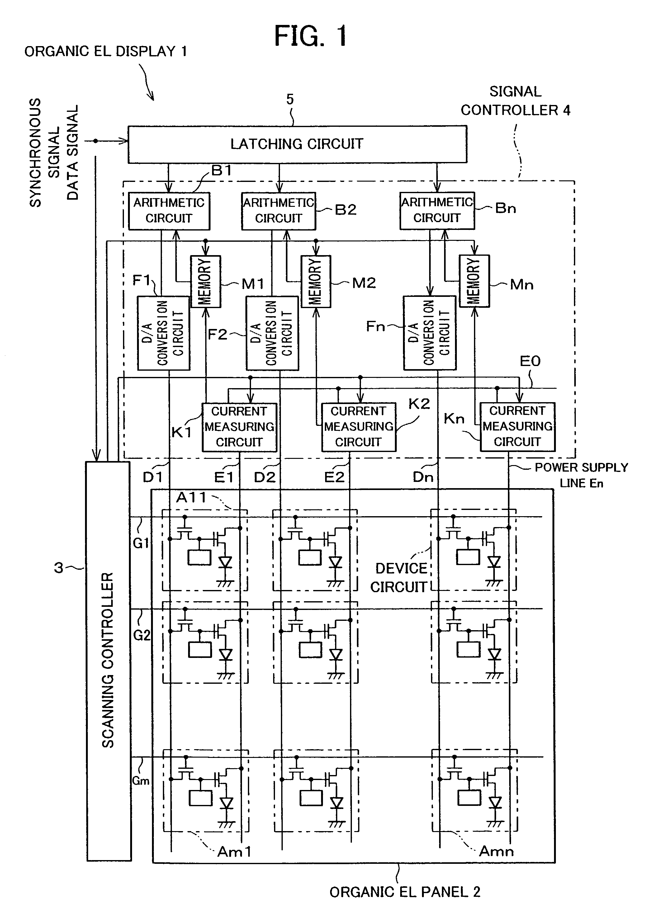
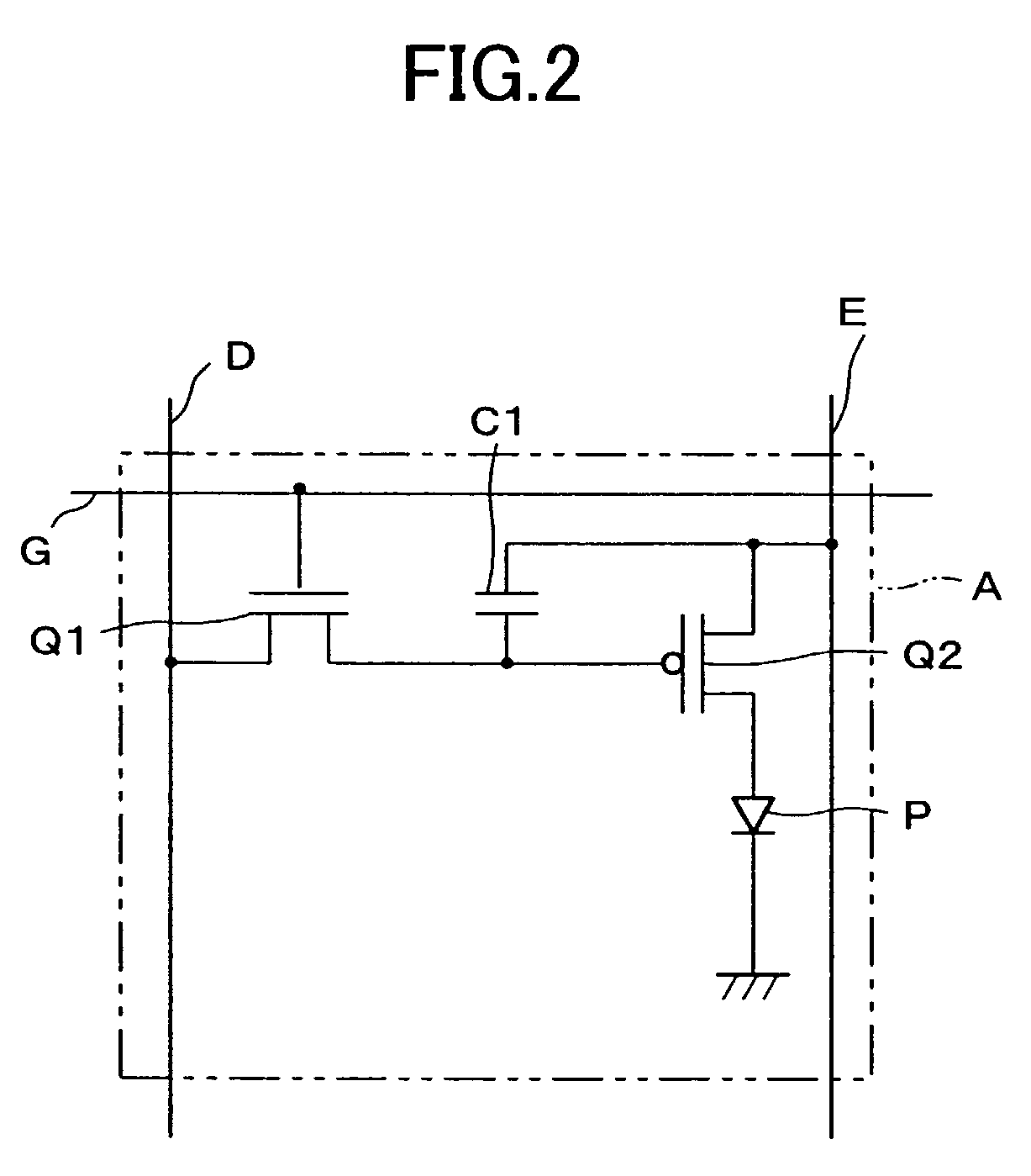
[0074]FIG. 1 illustrates an overall arrangement of an organic EL display 1 in accordance with the first embodiment of the present invention. The organic EL display 1 is basically composed of an organic EL panel 2, a scanning controller 3, a signal controller 4, and a latching circuit 5. The organic EL panel 2 is partitioned by: (i) scanning signal lines G1, G2, . . . , Gm (collectively termed G) which are a plurality of first signal lines; and (ii) data signal lines D1, D2, . . . , Dn (collectively termed D) which are a plurality of second signal lines, the lines (i) and (ii) intersecting with each other, and in the partitioned areas arranged in a matrix manner, device circuits A11, A12, . . . , A1n; A21, . . . , Amn (collectively termed A) are formed. While the scanning controller 3 is selecting a scanning signal line G, the corresponding device circuits A capture...

second embodiment

[0084]The following description will discuss a second embodiment in accordance with the present invention in reference to FIGS. 5 to 7.

[0085]FIG. 5 illustrates an overall arrangement of an organic EL display 11 in accordance with the second embodiment of the present invention. This organic EL display 11 is similar to the above-mentioned organic EL display 1, and hence members having the same functions as those described in the first embodiment are given the same numbers so that the descriptions are omitted. It should be noted that while the above-mentioned organic EL display 1 adopts an analog gradation control, this organic EL display 11 adopts a digital gradation control. Thus as FIG. 5 shows, the organic EL display 11 includes memories Mal to Man (collectively termed Ma) instead of the arithmetic circuits B1 to Bn of the organic EL display 1, and in the memories Ma, multi-bit data in accordance with each pixel, the data being sent in a serial manner, is broken down into each para...

third embodiment

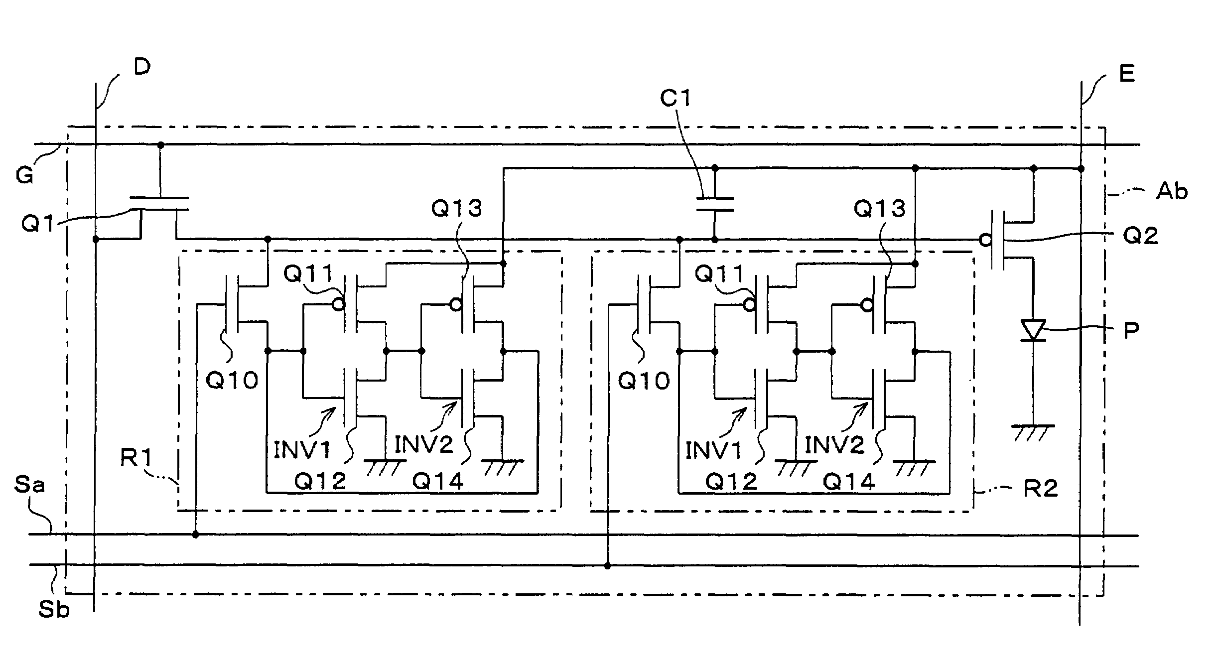
[0101]The following description will discuss a third embodiment in accordance with the present invention in reference to FIGS. 8 to 15.

[0102]FIG. 8 illustrates an overall arrangement of an organic EL display 21 in accordance with the third embodiment of the present invention. FIG. 9 is an electric circuit diagram illustrating a device circuit Ab in an organic EL panel 2b of the organic El display 21. This organic EL display 21 is similar to the above-mentioned organic EL displays 1 and 11, and hence members having the same functions as those described are given the same numbers so that the descriptions are omitted.

[0103]This organic EL display 21 adopts a special scanning method as below, so prior to the description of this method, the above-mentioned scanning method in FIG. 7 will be described in detail. The scanning method in FIG. 7 is arranged so that scanning time necessary for the time-division gradation display for 4 bits is: 7 units (a single scanning period)×5 units (=for 4 ...


PUM


Abstract

A display apparatus conducting time-division gradation display is provided with: a capacitor for keeping a signal level captured by a first TFT; at least one pixel memory, for keeping the signal level captured by the first TFT; a second TFT matched with the corresponding pixel memory; and a bit selecting line for selectively-driving the second TFT, wherein, when a scanning signal line is selected, the first TFT sets the display signal level is set in the capacitor via the first TFT and the second TFT is selectively driven so that the display signal level is set in the at least one pixel memory, whereas the TFT is selectively driven so that a display signal level which has been displayed is switched to the display signal level supplied from the at least one pixel memory.

Description

FIELD OF THE INVENTION[0001]The present invention relates to a display apparatus composed of electro-optical devices such as an organic EL (Electro Luminescence) device and an FED (Field Emission Device) being arranged in a matrix manner.BACKGROUND OF THE INVENTION[0002]Recently thin display apparatuses using self-luminous devices such as an organic EL device and an FED have actively been developed. It is known that the self-luminous devices have characteristics such that the luminance of the device is proportional to the current density of the current passing through the device. It is also known that the characteristics of the devices, especially the characteristics of the applied voltage-current fluctuate so that a drive circuit using a constant current source is preferably used for the devices. However, it is difficult to construct the constant current source in reality and hence a constant current drive circuit is arranged using a constant voltage source. For this case, a propos...

Claims


Application Information

Patent Timeline
IPC IPC(8): G09G3/30G09G3/00G09G3/10G09G3/12G09G3/20G09G3/22G09G3/32
CPCG09G3/3233G09G3/3258G09G3/2022G09G2320/043G09G2300/0842G09G2300/0857G09G2300/0876G09G2310/0205G09G2310/0251G09G2310/0262G09G2310/027G09G2320/0285G09G2320/029G09G2320/0295G09G3/22G09G3/30
Inventor NUMAO, TAKAJI
Owner SHARP KK
Why Eureka
Try Eureka