Semiconductor memory device

a memory device and semiconductor technology, applied in the field of semiconductor memory devices, can solve the problems of insufficient write, difficult shortening the read time and reducing electro-magnetic noise, and the threshold voltage of the memory cell appears to be varied,

Inactive Publication Date: 2006-03-07
KK TOSHIBA
View PDF12 Cites 181 Cited by
  • Summary
  • Abstract
  • Description
  • Claims
  • Application Information

AI Technical Summary

Benefits of technology

[0028]in the data read mode, the more unselected memory cell or cells located on the source side of the selected memory cell, the higher the pass voltage applied to the unselected memory cell or cells located on the source side of the selected memory cell.

Problems solved by technology

Further, since data read is based on detecting the charge amount flowing through the memory cells, there is a problem that the memory cell's threshold voltage appears to be varied.
On the other hand, if the read current of a logical data varies in accordance with a selected memory cell' position and data states of unselected memory cells, it becomes difficult to shorten a read time and reduce electro-magnetic noises due to the read current.
Further, as the read current of the selected cell becomes larger, the common source line SL is more boosted in potential, and this leads to a trouble that “0” data write is not sufficiently done in case write and verify-read are repeated (for example, refer to Published and Unexamined Japanese Patent Application No. 11-260076).
This leads to increasing the probability of erroneous read such as to read out “1” data as “0” data.
However, this leads to another problem.
Therefore, if the “0” data threshold voltage distribution is brought to a too high voltage range, it becomes difficult to secure a sufficient data retention property.
This causes data disturbance, erroneous read and the like.

Method used


Image

  • Semiconductor memory device
  • Semiconductor memory device
  • Semiconductor memory device

Examples


embodiment 1

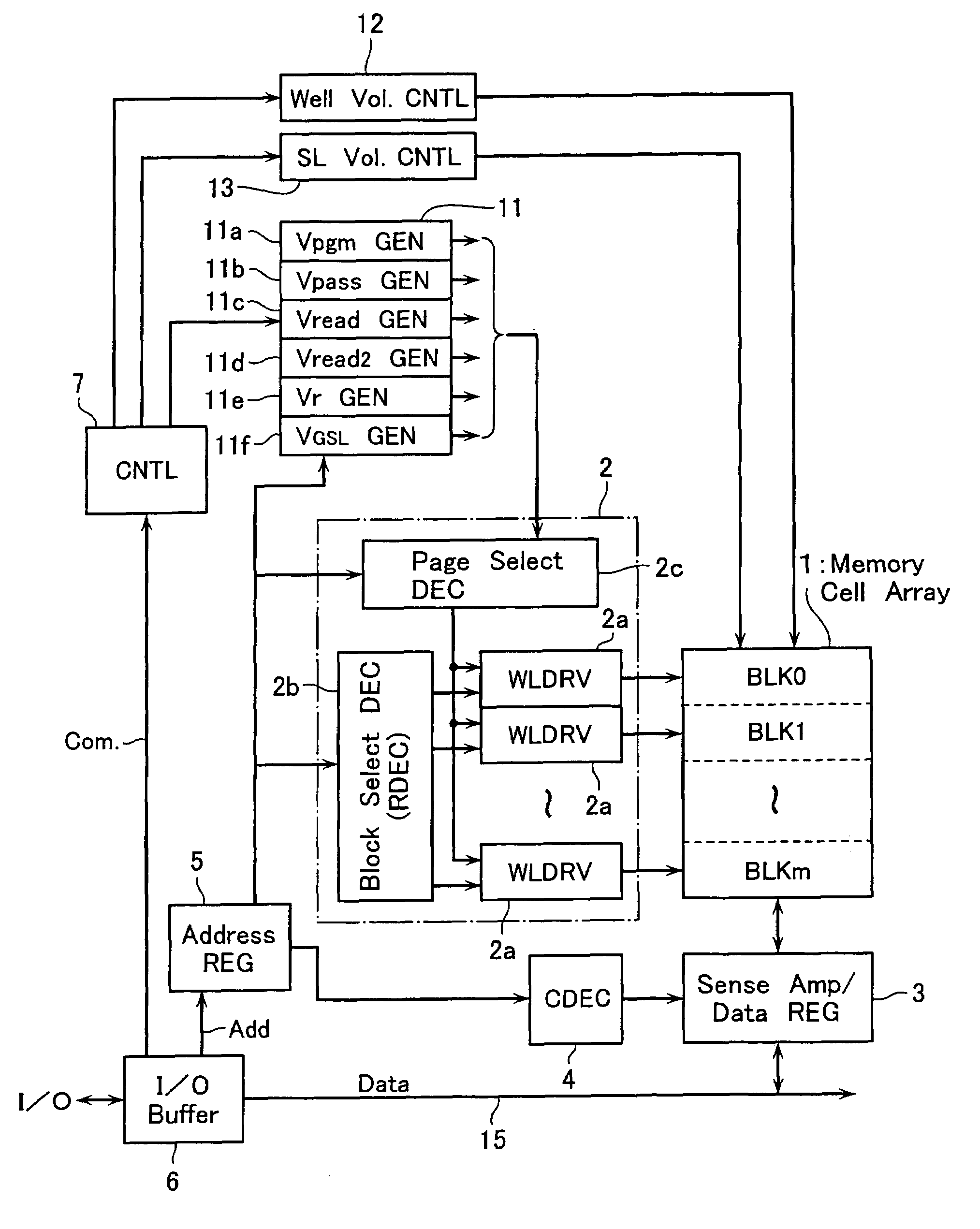
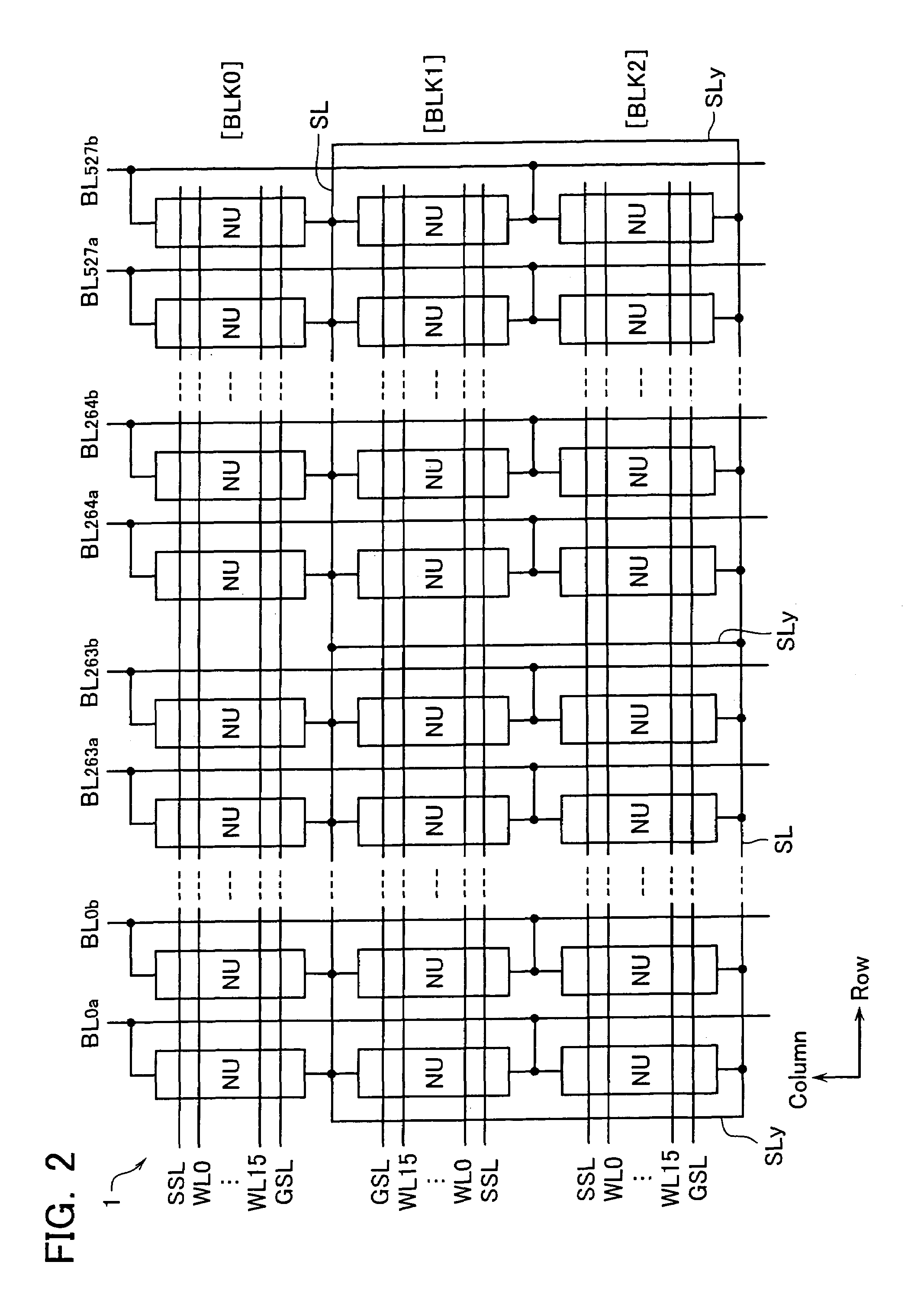
[0056]FIG. 1 shows a functional block configuration of a NAND-type EEPROM in accordance with an embodiment 1. FIGS. 2 and 3 show the memory cell array 1 and sense amplifier circuit 3 connected to it, respectively. The cell array 1 is formed of memory cell units (i.e., NAND cell units) NU arranged in row and column directions, each of which has a plurality of memory cells connected in series.

[0057]Each NAND cell unit NU is connected between a data transfer line BL (refers to as a “bit line” hereinafter) elongated in the column direction and a reference potential line SL (refers to as a “common source line” hereinafter) elongated in the row direction. Data control lines (refers to as “word lines” hereinafter) WL(WL0–WL15) for selectively driving memory cells in the NAND cell unit NU and select gate lines SSL, GSL for block selecting are disposed common to the NAND cell units MU arranged in the row direction.

[0058]To sense bit line data of the memory cell array 1 and to hold a write da...

embodiment 2

[0156]Next, another embodiment 2 will be explained, in which the read current is carried from the common source line SL to the bit line BL in contrast to the above-described embodiment 1. The EEPROM configuration shown in FIG. 1 to FIG. 6C and the Vread generator shown in FIGS. 9 and 10 are used as there are in this embodiment 2.

[0157]FIG. 14 shows a data read timing chart in this embodiment 2, which corresponds to that shown in FIG. 7 in the embodiment 1. An example of the pass voltage Vread set in this embodiment is shown in FIGS. 15A to 15D, and FIGS. 16 and 17 which correspond to FIGS. 8A to 8D, and FIGS. 12 and 13, respectively, in the above-described embodiment.

[0158]In this embodiment, a memory cell coupled to one bit line BLxb within the bit lines BLxa and BLxb shown in FIGS. 2 and 3 is subjected to data read by the sense amplifier, and the other, unselected bit line BLxa is fixed in potential at substantially the same level as the source line SL so as to serve as a shield l...

embodiment 3

[0187]EEPROM flash memories in accordance with the above-described embodiments may be adapted to various applications such as flash memory cards installed detachable to various electric devices, and other flash memory systems.

[0188]FIG. 23 shows a flash memory system, which is another application example of the EEPROM chip incorporating the principles of any one of the embodiments 1 and 2 stated supra. This flash memory system is generally made up of a host platform 601 and its associated universal serial bus (USB) flash device 602. The host platform 601 is connected to the USB flash device 602 through a USB cable 605. Host platform 601 is connected by a USB host connector 604 to USB cable 605. USB flash device 602 is connected to USB cable 605 via a USB flash device connector 606.

[0189]The host platform 601 has a USB host controller 603 for controlling packet data transmission over a USB bus(es). The USB flash device 602 has at least one flash memory module 608 and a USB flash devi...


PUM


Abstract

A semiconductor memory device includes a memory cell unit with a plurality of electrically rewritable memory cells connected in series, two ends thereof being coupled to a data transfer line and a reference potential line via select transistors, respectively, wherein the device has a data read mode defined as to detect a read current flowing between the data transfer line and the reference potential line, and judge data of a selected memory cell in the memory cell unit under the condition of: applying a read voltage to the selected memory cell, the read voltage being set to turn on or off the selected memory cell in accordance with data thereof; applying a pass voltage to remaining unselected memory cells, the pass voltage being set to turn on the remaining unselected memory cells without regard to data thereof; and making the select transistors on, and wherein in the data read mode, the more unselected memory cell or cells located on the source side of the selected memory cell, the higher the pass voltage applied to the unselected memory cell or cells located on the source side of the selected memory cell.

Description

CROSS-REFERENCE TO RELATED APPLICATION[0001]This application is based on and claims the benefit of priority from the prior Japanese Patent Application No. 2004-146112, filed on May 17, 2004, the entire contents of which are incorporated herein by reference.BACKGROUND OF THE INVENTION[0002]1. Field of the Invention[0003]This invention relates to a semiconductor memory device in which a plurality of memory cells are connected in series to constitute a memory cell unit.[0004]2. Description of Related Art[0005]A memory cell in an EEPROM has usually a MISFET structure which is formed of a semiconductor substrate with a charge storing layer and a control gate stacked thereabove. This memory cell stores data in a non-volatile manner, as defined by a threshold state in which charges are injected into the charge storing layer and another threshold state in which the charges have been released. The charge injecting / releasing is done by a tunneling current trough a tunnel insulating film betwe...

Claims


Application Information

Patent Timeline
Patent Type & Authority Patents(United States)
IPC IPC(8): G11C16/00G11C16/06G11C11/34G11C16/04G11C16/08
CPCG11C16/08G11C16/0483G11C16/26G11C16/30
Inventor NOGUCHI, MITSUHIRO
Owner KK TOSHIBA
Why Eureka
Try Eureka