Scalable flash/NV structures and devices with extended endurance

a flash/nv technology, applied in the field of integrated circuits, can solve the problems of limited endurance of flash/nv devices, limited progress of scaling flash/nv programming voltage and power, and devices that are capable of performing a limited number of write/erase cycles, so as to extend the scalability of nv technology, improve endurance, and reduce programming field

Inactive Publication Date: 2006-03-14
MICRON TECH INC
View PDF49 Cites 148 Cited by
  • Summary
  • Abstract
  • Description
  • Claims
  • Application Information

AI Technical Summary

Benefits of technology

[0010]The above mentioned problems are addressed by the present subject matter and will be understood by reading and studying the following specification. The present subject matter provides a scalable Flash / NV structure that further extends the scalability of NV technology by providing a gate stack with a high K dielectric, a charge center or charge storing medium and at least one charge injector medium. The present subject matter requires a lower programming field, improves endurance, achieves faster write-erase cycles, and has variables that are capable of being manipulated for scaling purposes.
[0011]One aspect is a gate stack for a nonvolatile device. According to one embodiment, the gate stack includes a tunnel medium, a high K charge blocking and charge storing medium, and an injector medium. According to this embodiment, the high K charge blocking and charge storing medium is disposed on the tunnel medium. Also according to this embodiment, the injector medium is operably disposed with respect to the tunnel medium and the high K charge blocking and charge storing medium to provide charge transport by enhanced tunneling. According to one embodiment, the injector medium is disposed on the high K charge blocking and charge storing medium. According to one embodiment, the tunnel medium is disposed on the injector medium.

Problems solved by technology

However, the progress of scaling Flash / NV programming voltage and power has been limited.
Additionally, the Flash / NV devices have a limited endurance.
That is, these devices are capable of performing a limited number of write / erase cycles that prevent their use in a number of applications.
The progress of extending the endurance of Flash / NV devices also has been limited.
As such, the integration of NV devices with general high performance logic technology and DRAM technology is complicated.
Additionally, the endurance of these NV devices is limited to about 10E5-10E6 cycles.
Therefore, providing embedded Flash / EPROM in a general random logic or DRAM environment to achieve enriched functions requires complex circuitry and many additional masks, resulting in a relatively limited yield and high cost.
However, the write / erase fields were still too high, and both the endurance and power reductions were still too limited.
While somewhat reduced voltage write / erase and up to 10E6 endurance were demonstrated, the write / erase fields were still too high, and both the endurance and the power reductions were still too limited.

Method used


Image

  • Scalable flash/NV structures and devices with extended endurance
  • Scalable flash/NV structures and devices with extended endurance
  • Scalable flash/NV structures and devices with extended endurance

Examples


Embodiment Construction

[0045]The following detailed description of the invention refers to the accompanying drawings which show, by way of illustration, specific aspects and embodiments in which the invention may be practiced. In the drawings, like numerals describe substantially similar components throughout the several views. These embodiments are described in sufficient detail to enable those skilled in the art to practice the invention. Other embodiments may be utilized and structural, logical, and electrical changes may be made without departing from the scope of the present invention. The following detailed description is, therefore, not to be taken in a limiting sense, and the scope of the present invention is defined only by the appended claims, along with the full scope of equivalents to which such claims are entitled.

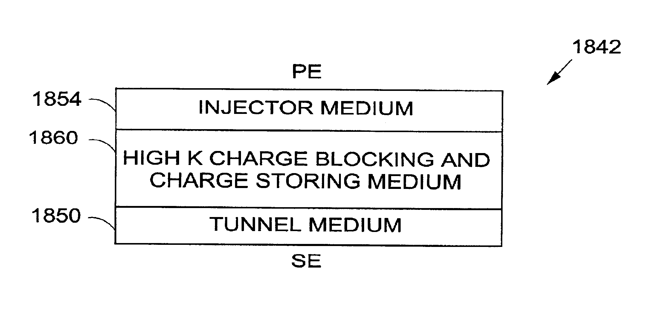
[0046]The present subject matter provides a scalable Flash / NV structure that further extends the scalability of NV technology by providing a gate stack with a high K dielectric, a c...


PUM


Abstract

Devices and methods are provided with respect to a gate stack for a nonvolatile structure. According to one aspect, a gate stack is provided. One embodiment of the gate stack includes a tunnel medium, a high K charge blocking and charge storing medium, and an injector medium. The high K charge blocking and charge storing medium is disposed on the tunnel medium. The injector medium is operably disposed with respect to the tunnel medium and the high K charge blocking and charge storing medium to provide charge transport by enhanced tunneling. According to one embodiment, the injector medium is disposed on the high K charge blocking and charge storing medium. According to one embodiment, the tunnel medium is disposed on the injector medium. Other aspects and embodiments are provided herein.

Description

TECHNICAL FIELD OF THE INVENTION[0001]This invention relates generally to integrated circuits and, more particularly, to nonvolatile programmable memory cells and reprogrammable logic circuit elements.BACKGROUND OF THE INVENTION[0002]General CMOS silicon gate technology has been scaled rapidly from the 1.0 μm generation (VDD=5.0 V) to the 0.13 μm generation (VDD=1.5 V) over a period of little over a decade. However, the progress of scaling Flash / NV programming voltage and power has been limited. Additionally, the Flash / NV devices have a limited endurance. That is, these devices are capable of performing a limited number of write / erase cycles that prevent their use in a number of applications. The progress of extending the endurance of Flash / NV devices also has been limited.[0003]Most NV devices have a floating gate and use a power hungry channel hot electron write process and a tunnel erase process through the tunnel oxide. The tunnel erase process requires both a high programming v...

Claims


Application Information

Patent Timeline
Patent Type & Authority Patents(United States)
IPC IPC(8): H01L29/788H01L21/28H01L29/423H01L29/51H01L29/792
CPCB82Y10/00H01L29/792G11C16/0466H01L21/28194H01L21/28273H01L21/28282H01L29/42332H01L29/513H01L29/518H01L29/66825H01L29/66833H01L29/7881G11C16/0416G11C2216/06H01L29/517H01L29/40114H01L29/40117
Inventor BHATTACHARYYA, ARUP
Owner MICRON TECH INC
Why Eureka
Try Eureka