Resistance multiplier circuit and compact gain attenuator

a technology of resistive multiplier circuit and compact gain attenuator, which is applied in the direction of one-port active network, multiple-port active network, ac network voltage adjustment, etc., and can solve the problems of high-value resistances that are difficult to achiev

Active Publication Date: 2006-03-14
MICREL
View PDF3 Cites 2 Cited by
  • Summary
  • Abstract
  • Description
  • Claims
  • Application Information

AI Technical Summary

Benefits of technology

[0006]According to one embodiment of the present invention, a circuit coupled to a first node of a first circuit includes a first transistor, a second transistor being N times larger than the first transistor, and a resistor for providing a resistance value at the first node that is a multiple of the resistance value of the resistor. The first transistor has a control terminal and a first curr

Problems solved by technology

Directly creating such a high-value resistance element may be either unfeasible or undesirable due to tradeoffs that need to be made in performance and/or size of such a resistance element.
While using the NPN base region offers the best accuracy and best thermal and voltage coefficients, typical resistivities are so low as to make high-value resistances very area-consuming.
Not only is the area consumed by 250 squares significant, but the capacitance associated with the resulting resistance element is undesirably large, causing signific

Method used


Image

  • Resistance multiplier circuit and compact gain attenuator
  • Resistance multiplier circuit and compact gain attenuator
  • Resistance multiplier circuit and compact gain attenuator

Examples


Embodiment Construction

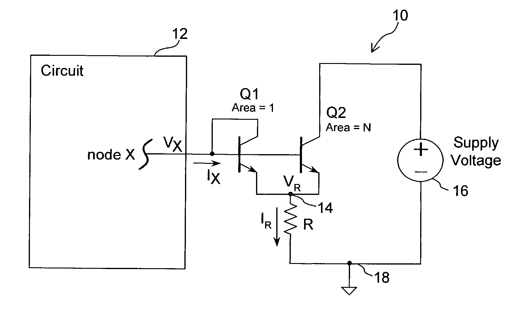
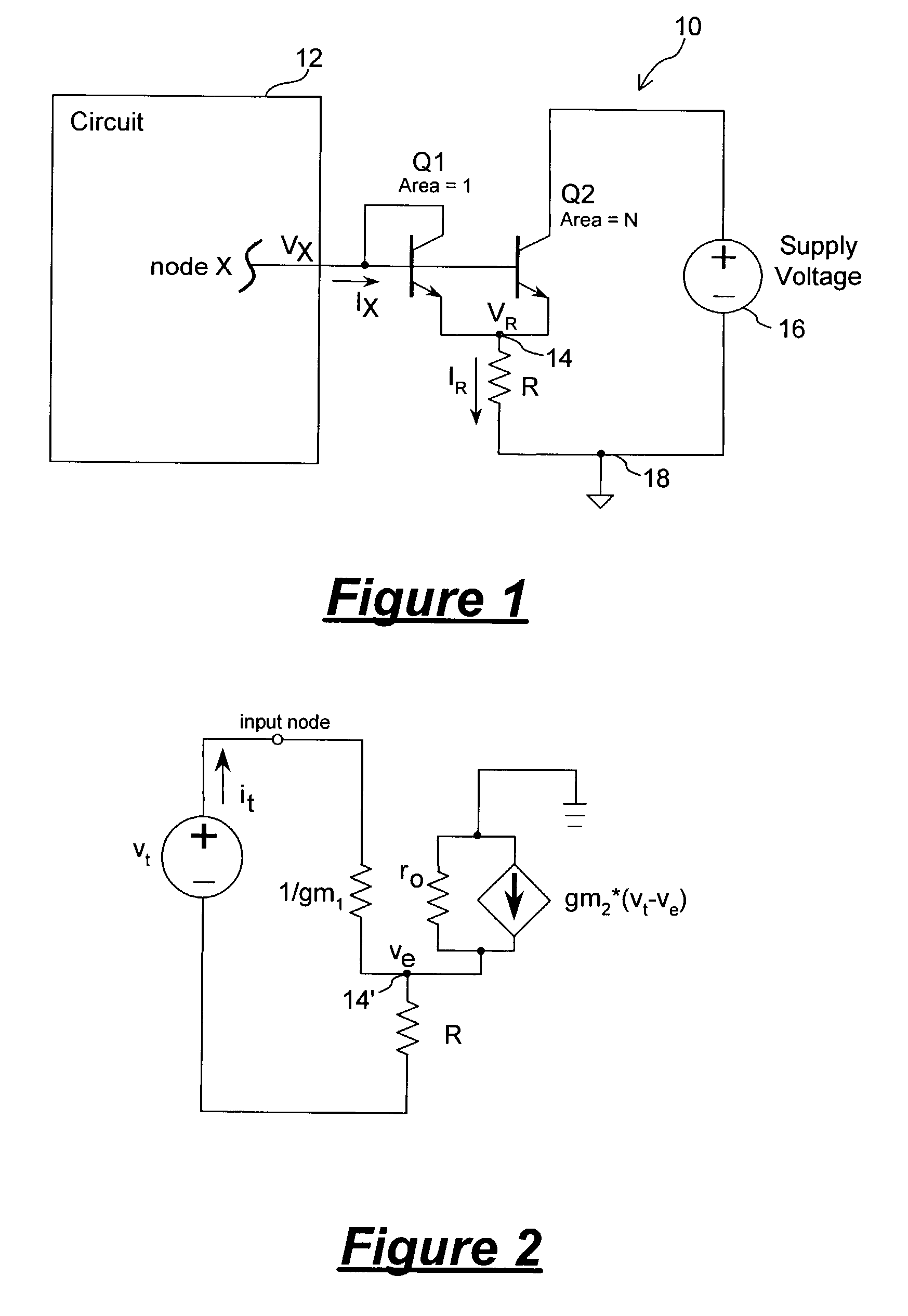
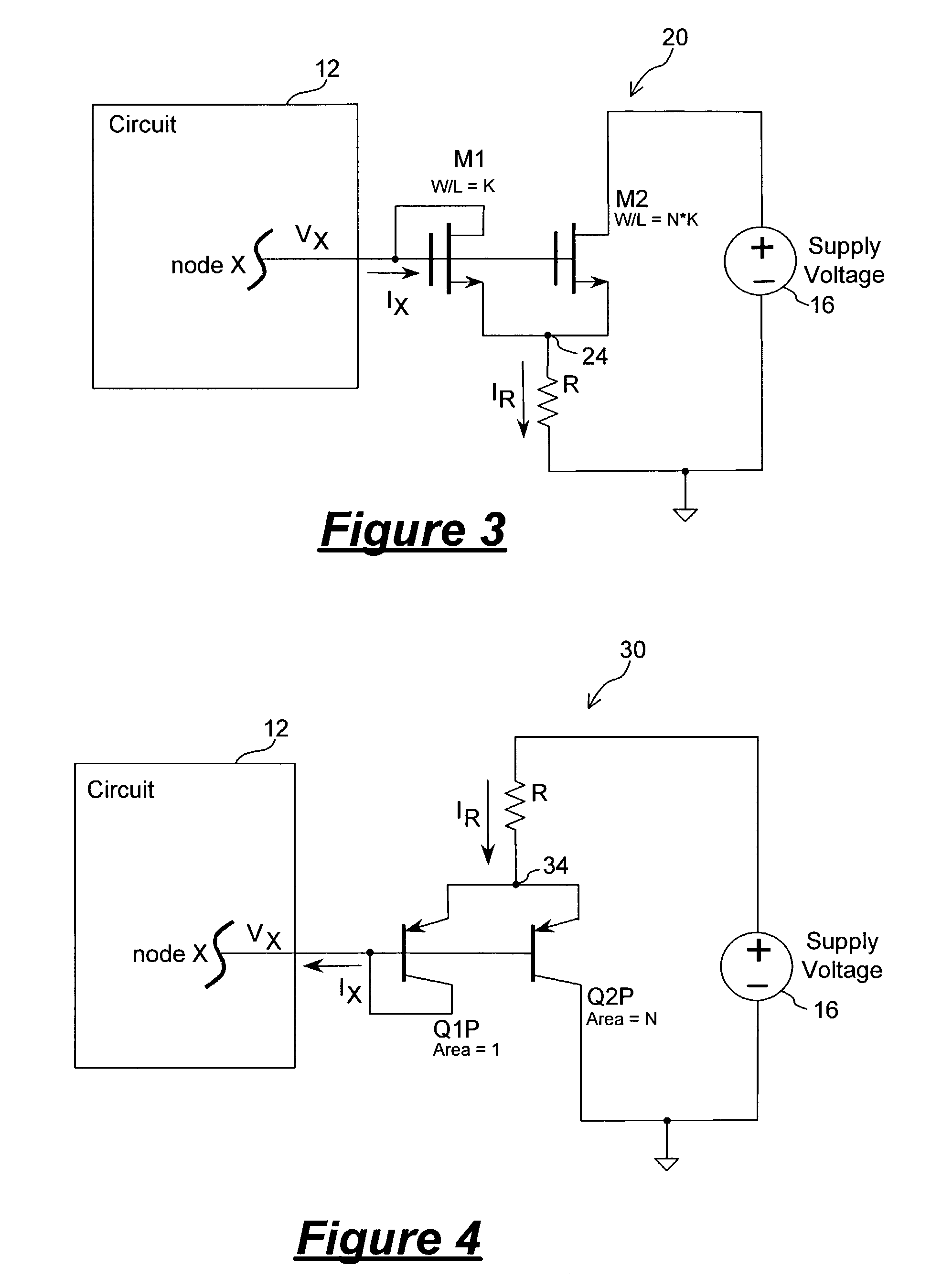
[0017]In accordance with the principles of the present invention, a circuit for providing a high-value resistance to a first node uses active circuitry to multiply the resistance value of a resistor. In this manner, a high-value resistance can be provided in an integrated circuit by using a comparatively small structure. In one embodiment, the resistance multiplier circuit includes a pair of unevenly sized transistors coupled to the first node and to a resistor. The transistors are configured as a current mirror for drawing currents through the resistor. By discarding part of the current drawn, the resistance value as seen from the first node can be made larger than actual resistance of the resistor itself. The geometric ratio of the pair of transistors establishes the amount of resistance multiplication that can be realized.

[0018]The resistance multiplier circuit of the present invention offers many advantages. First, the resistance multipler circuit including two transistors requi...


PUM


Abstract

A resistance multiplier circuit coupled to a first node of a first circuit for providing a high-value resistance at the first node includes a first transistor, a second transistor being N times larger than the first transistor, and a resistor. In one embodiment, the first and second transistors are NPN bipolar transistors. The first transistor has its base and collector terminals coupled to the first node and an emitter terminal coupled to a second node. The second transistor has a base terminal coupled to the first node, a collector terminal coupled to a positive supply voltage, and an emitter terminal coupled to the second node. The resistor is coupled between the second node and a virtual ground node. When a voltage is applied to the first node, the resistance at the first node is (N+1) times the resistance of the resistor.

Description

FIELD OF THE INVENTION[0001]The invention relates to a circuit for providing a high-value resistance in an integrated circuit and, in particular, to a circuit for multiplying the resistance value of a resistor so that a high-value resistance can be provided in less area and with stable operation characteristics.DESCRIPTION OF THE RELATED ART[0002]In integrated circuit designs, a high-value resistance is often needed. Directly creating such a high-value resistance element may be either unfeasible or undesirable due to tradeoffs that need to be made in performance and / or size of such a resistance element. For example, one conventional method for realizing high-value resistances in an integrated circuit includes using a silicon resistance such as the base region of an NPN bipolar transistor to form the resistance element. While using the NPN base region offers the best accuracy and best thermal and voltage coefficients, typical resistivities are so low as to make high-value resistances...

Claims


Application Information

Patent Timeline
IPC IPC(8): H02J1/00H03H11/24H03H11/40H03H11/46
CPCH03H11/24H03H11/53H03H11/46
Inventor INN, BRUCE L.WENG, MATTHEW
Owner MICREL
Why Eureka
Try Eureka