Semiconductor device driving bridge-connected power transistor

a technology of power transistor and semiconductor device, which is applied in the direction of transistor, electronic switching, pulse technique, etc., can solve the problems of reducing the potential at the bootstrap power supply node (vb) by the decouple capacitor, causing a spike-like noise, and affecting the operation of high-speed switching

Active Publication Date: 2010-11-11
MITSUBISHI ELECTRIC CORP
View PDF0 Cites 44 Cited by
  • Summary
  • Abstract
  • Description
  • Claims
  • Application Information

AI Technical Summary

Benefits of technology

[0019]The foregoing and other objects, features, aspects and advantages of the present invention will become more appar...

Problems solved by technology

In a bridge configuration, when the load is an inductive load, a spike-like noise is generated by the current flowing through the free-wheel diode of the low-side power transistor when the high-side power transistor is turned off.
However, generation of a negative spike-like noise at the virtual ground node (VS) causes reduction in the potential at the bootstrap power supply node (VB) by the decouple capacitor.
Furthermore, th...

Method used


Image

  • Semiconductor device driving bridge-connected power transistor
  • Semiconductor device driving bridge-connected power transistor
  • Semiconductor device driving bridge-connected power transistor

Examples


first embodiment

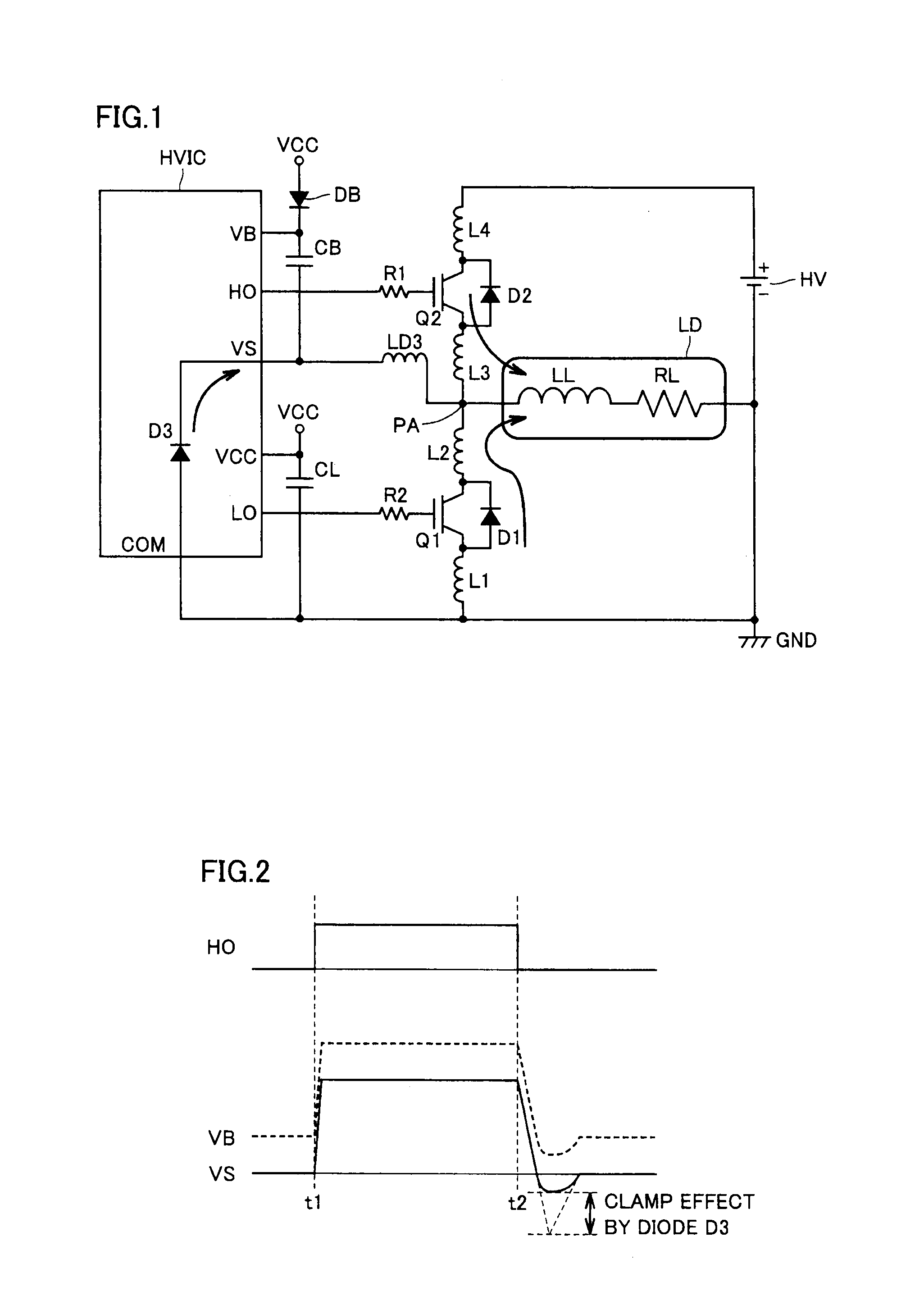
[0036]Referring to FIG. 1, a high-voltage control circuit (semiconductor device) HVIC sets the ON / OFF of a low-side power transistor Q1 and a high-side power transistor Q2. By way of example, power transistors Q1 and Q2 are formed of an IGBT (Insulated Gate Bipolar Transistor), having free-wheel diodes D1 and D2 connected in parallel in the reverse direction between the drain and source.

[0037]A high voltage supply HV is provided as the power supply for power transistors Q1 and Q2. High voltage supply HV has a positive electrode coupled to a drain node of power transistor Q2, and a negative electrode coupled to a source node of power transistor Q1. Parasitic inductance components L1-L4 are present at the drain and source interconnections of power transistors Q1 and Q2.

[0038]A load circuit LD is connected between a connection node (hereinafter, referred to as intermediate node) PA of power transistors Q1 and Q2 and the negative electrode of the high voltage supply. By way of example, ...

second embodiment

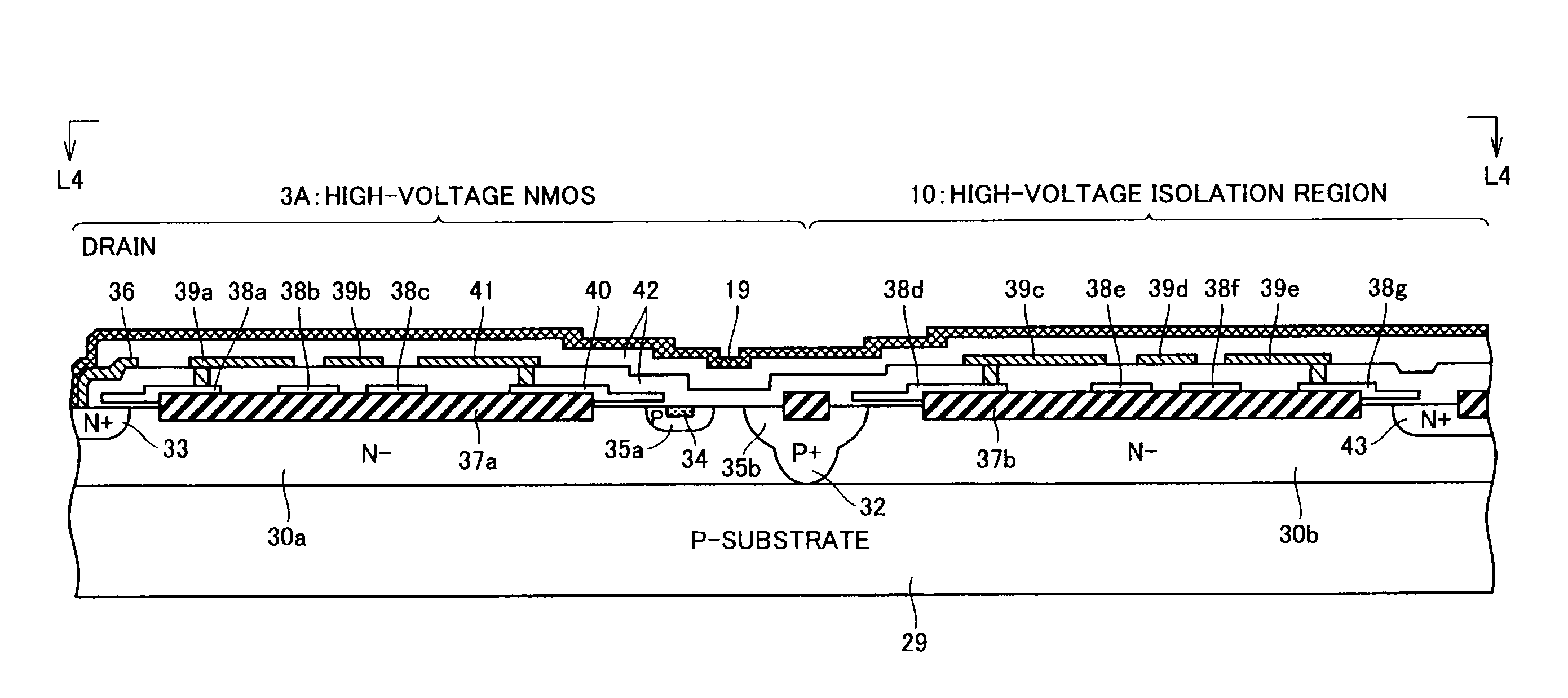
[0099]FIG. 8 schematically shows a plan layout of a high-voltage control circuit HVIC according to the second embodiment of the present invention. In the configuration of high-voltage control circuit HVIC shown in FIG. 8, a high-voltage diode for VS clamping is formed taking advantage of high-voltage isolation region 10 located in high-voltage potential island region 9 where high-side logic circuit 2 is formed. Specifically, in high-voltage isolation region 10, an anode electrode 70 of high-voltage diode D3 for clamping is formed extending continuously along the entire perimeter of high-voltage isolation region 10 to take a track-like shape. A cathode electrode 72 is formed continuously in a track-like shape within high-voltage isolation region 10. A slit region 74 is located between cathode electrode 72 and high-side logic circuit region 76. By this slit region 74, the N type semiconductor layer constituting high-voltage diode D3 and the N type semiconductor layer constituting high...

third embodiment

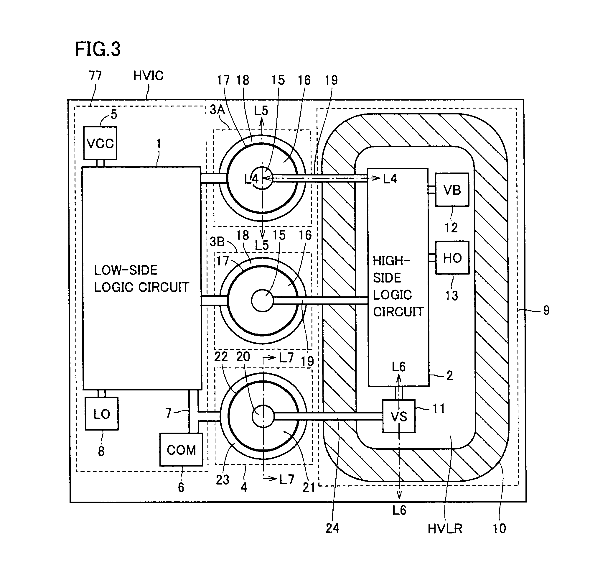
[0111]FIG. 10 schematically represents a plan layout of a high-voltage control circuit HVIC according to a third embodiment of the present invention. At high-voltage control circuit HVIC of FIG. 10, common ground pad 6 coupled to common ground node COM is connected to low-side logic circuit 1 via internal interconnection 7A. Ground voltage GND from common ground node COM is supplied to P type semiconductor substrate 29 where high-voltage control circuit HVIC is formed.

[0112]The high-voltage diode for VS clamping is formed at virtual ground potential pad 11 that supplies virtual ground voltage VS. Cathode electrode region 88 is formed at this virtual ground potential pad 11. A slit region 86 is formed at the outer perimeter of cathode electrode region 88 to isolate the N type impurity region to which virtual ground pad 11 is coupled from the N type semiconductor layer constituting the substrate region for high-side logic circuit formation region 76 (high-voltage potential island regi...


PUM


Abstract

A semiconductor device includes a low-side circuit, high-side circuit, a virtual ground potential pad, a common ground potential pad and a diode, formed on a semiconductor substrate. The low-side circuit drives a low-side power transistor. The high-side circuit is provided at a high potential region, and drives a high-side power transistor. The virtual ground potential pad is arranged at the high potential region, and coupled to a connection node of both power transistors to supply a virtual ground potential to the high-side circuit. The common ground potential pad supplies a common ground potential to the low-side circuit and high-side circuit. The diode has its cathode connected to the virtual ground potential pad and its anode connected to the common ground potential pad.

Description

BACKGROUND OF THE INVENTION[0001]1. Field of the Invention[0002]The present invention relates to a semiconductor device driving a bridge-connected power device in a push-pull manner.[0003]2. Description of the Background Art[0004]A power device of an IGBT (Insulated-Gate Bipolar Transistor) that handles large power is widely used in applications of driving a power motor and the like. A power device (power transistor) is often used in the form of a half-bridge circuit having two power devices driving a load alternately, or an H bridge circuit having four power transistors driving a load alternately.[0005]Such power devices are required to switch more current at high speed. Problems occurring by the parasitic inductance of a bridge circuit in switching high-amperage current at high speed and a method for improving such problem are disclosed in Non-Patent Document 1 (“Solving the Problem of Noise When Driving at High Power and High Frequency by Power IC” by L. Kiraly in International R...

Claims


Application Information

Patent Timeline
IPC IPC(8): H01L27/06
CPCH01L21/76202H01L21/823481H01L23/5225H01L24/05H01L24/48H01L27/0629H01L29/0696H01L29/402H01L29/42368H01L29/7816H01L29/8611H01L2224/04042H01L2224/05599H01L2224/48247H01L2224/48465H01L2224/49171H01L2924/01004H01L2924/01011H01L2924/01013H01L2924/01014H01L2924/01015H01L2924/01032H01L2924/01033H01L2924/01046H01L2924/0106H01L2924/01074H01L2924/01082H01L2924/014H01L2924/13055H01L2924/13091H01L2924/14H01L2924/19041H01L2924/30107H01L2924/3025H02M7/003H03K17/161H01L24/49H01L2924/01006H01L2924/01023H01L2924/01041H01L2924/01067H01L2924/01068H01L2924/00014H01L2224/05556H01L2924/1306H01L2924/12032H01L2924/1305H01L2924/00H01L2924/12036H01L2924/12041H01L2224/45099
Inventor SHIMIZU, KAZUHIRO
Owner MITSUBISHI ELECTRIC CORP
Why Eureka
Try Eureka