Segmented Column Virtual Ground Scheme In A Static Random Access Memory (SRAM) Circuit

a static random access memory and segmented column technology, applied in the direction of read-only memories, static storage, instruments, etc., can solve the problem of low power read operation, reduce the leakage current of memory cells, reduce the bit-line swing voltage, and reduce the power write operation

Inactive Publication Date: 2007-09-20
SACHDEV MANOJ +1
View PDF6 Cites 41 Cited by
  • Summary
  • Abstract
  • Description
  • Claims
  • Application Information

AI Technical Summary

Benefits of technology

[0008] Through the introduction of a segmented virtual grounding scheme, leakage current of the memory cells is reduced. Further, a reduced bit-line swing voltage enables lower power write operation. Yet further, this scheme inhibits discharging unselected bit-lines, which results in low power read operation.

Problems solved by technology

Yet further, this scheme inhibits discharging unselected bit-lines, which results in low power read operation.

Method used


Image

  • Segmented Column Virtual Ground Scheme In A Static Random Access Memory (SRAM) Circuit
  • Segmented Column Virtual Ground Scheme In A Static Random Access Memory (SRAM) Circuit
  • Segmented Column Virtual Ground Scheme In A Static Random Access Memory (SRAM) Circuit

Examples


Embodiment Construction

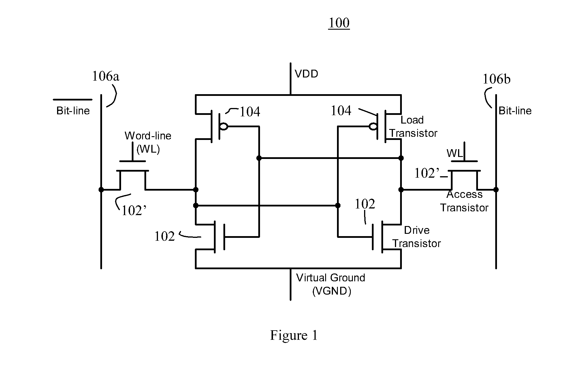
[0020] For convenience, like numerals in the description refer to like structures in the drawings. Referring to FIG. 1, a standard six-transistor SRAM cell is illustrated generally by numeral 100. The cell 100 comprises a pair of n-type drive transistors 102 and a pair of p-type load transistors 104 in a cross-coupled configuration. A further pair of n-type access transistors 102′ couples the cell 100 to a complementary bit-line pair 106a and 106b. The source of the drive transistors 104 is coupled to a virtual ground VGND and the source of the load transistors 102 is coupled to a supply voltage VDD.

[0021] The cell 100 is coupled to the bit-line pair 106a and 106b in a response to a word-line control signal WL from a row decoder (not shown). Accordingly, when the word-line control signal WL is active, the cell 100 is electrically connected to the bit-line pair 106a and 106b.

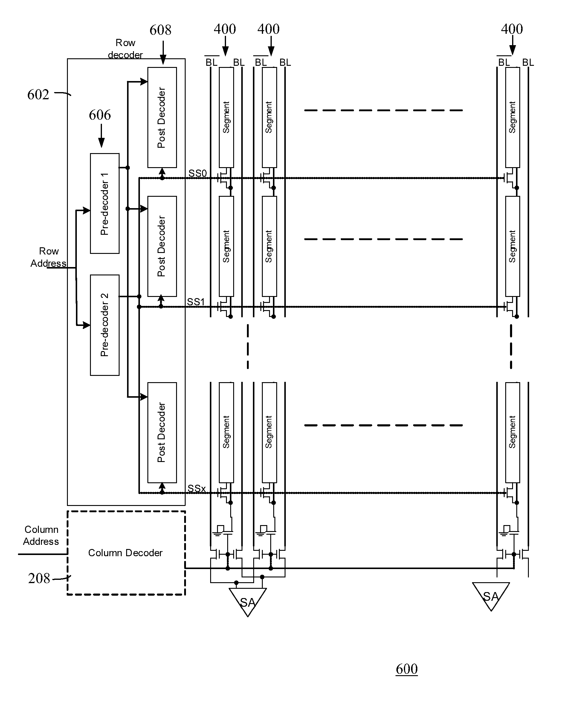
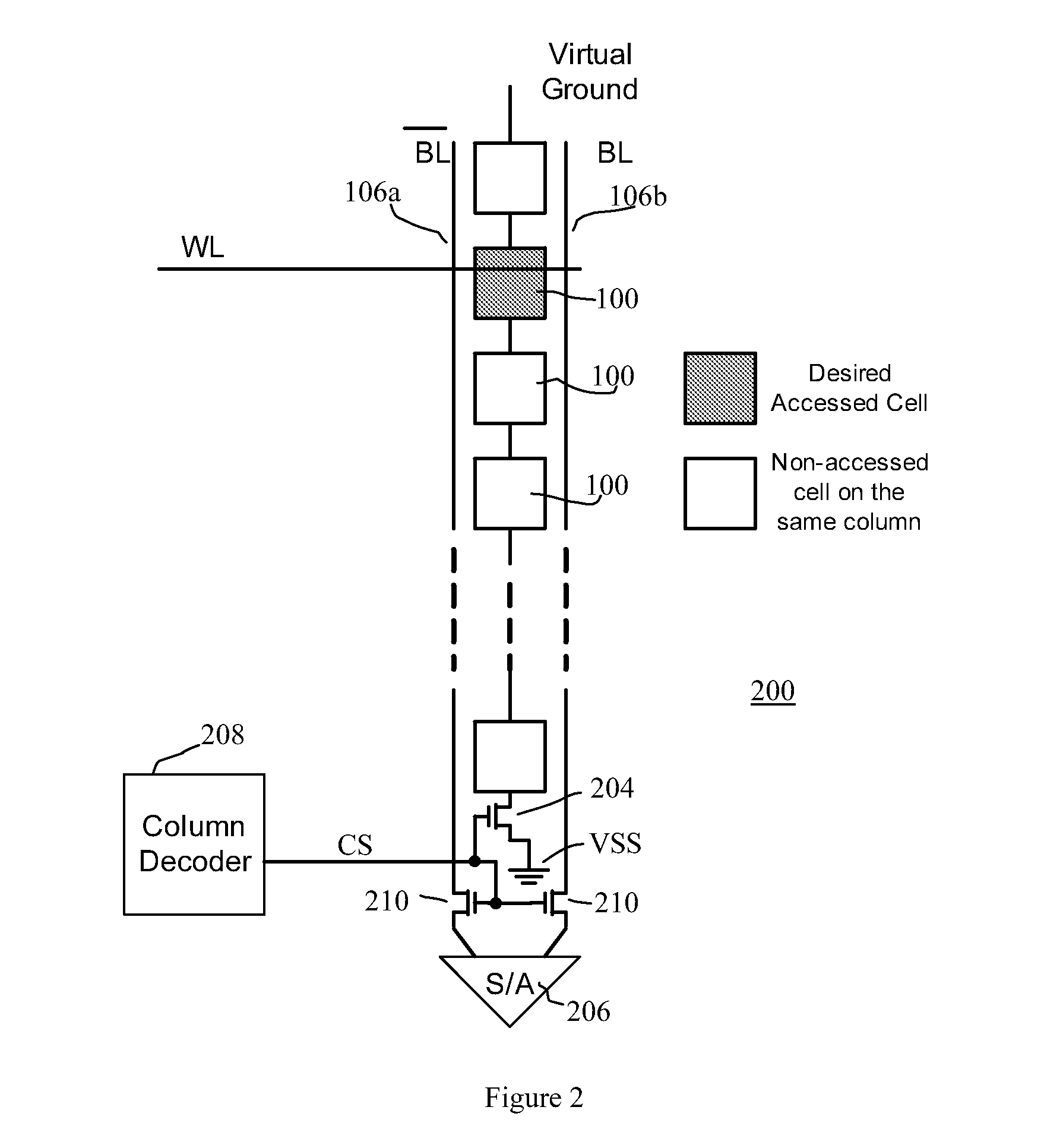
[0022] Referring to FIG. 2, a standard column of an SRAM block array using a virtual ground scheme is illust...


PUM


Abstract

A static random access memory (SRAM) cell array is provided that reduces leakage current. The SRAM cell array is configured in a plurality of columns. Each of the columns comprises: a column virtual ground node; a column switch for selectively coupling the column virtual ground node to one of a ground or a nominal low voltage; and a plurality of segments. Each of the segments comprises: a segment virtual ground node; a plurality of SRAM cells including a virtual ground signal coupled to the segment virtual ground node; and a virtual ground switch for selectively coupling the segment virtual ground node to one of either a nominal low voltage or the column virtual ground node. A method for operating the SRAM cell array is also described.

Description

[0001] The present invention relates generally to Static Random Access Memory (SRAM) cell arrays and specifically to a scheme that improves power performance of memory cells in the cell arrays. This application claims priority from U.S. Provisional Application No. 60 / 729,936, filed Oct. 26, 2005.BACKGROUND OF THE INVENTION [0002] Embedded memories have been a vital component of system-on-chip solutions for decades. However, memory blocks occupy a significant portion of the chip's die area, making it an important component in terms of area and power consumption. With increasing demand for battery-operated applications, methods for reducing power consumption of the memory blocks have received significant interest. In particular, static random access memory (SRAM) has been receiving a lot of attention. [0003] Six-transistor SRAM cells are preferred for many applications because of their high speed and small area. This configuration, however, suffers from high stand-by power consumption...

Claims


Application Information

Patent Timeline
Patent Type & Authority Applications(United States)
IPC IPC(8): G11C16/04
CPCG11C8/10G11C11/413G11C11/412G11C8/12
Inventor SACHDEV, MANOJSHARIFKHANI, MOHAMMAD
Owner SACHDEV MANOJ
Why Eureka
Try Eureka