Optical device with enhanced mechanical stability operating in the extreme ultraviolet and lithography mask comprising such a device

a technology of optical devices and mechanical stability, applied in the field of optical devices, can solve the problems of achieving the maximum value of theoretically, and achieve the effect of mechanical stress and maximum optical reflection

Inactive Publication Date: 2006-03-14
COMMISSARIAT A LENERGIE ATOMIQUE ET AUX ENERGIES ALTERNATIVES
View PDF6 Cites 12 Cited by
  • Summary
  • Abstract
  • Description
  • Claims
  • Application Information

AI Technical Summary

Benefits of technology

[0016]Another object of the invention is to achieve a lithography mask with stable mechanical stresses over time.

Problems solved by technology

It is however difficult to achieve this theoretical maximum value, notably due to an interdiffusion phenomenon taking place between the silicon and molybdenum.
However, for a lithography mask used in EUV for example, the maximum deformation allowed is 50 nm, which is not compatible with such a variation of mechanical stresses, the latter greatly conditioning the flatness of the optical wave front of the lithography mask.

Method used


Image

  • Optical device with enhanced mechanical stability operating in the extreme ultraviolet and lithography mask comprising such a device
  • Optical device with enhanced mechanical stability operating in the extreme ultraviolet and lithography mask comprising such a device
  • Optical device with enhanced mechanical stability operating in the extreme ultraviolet and lithography mask comprising such a device

Examples


Embodiment Construction

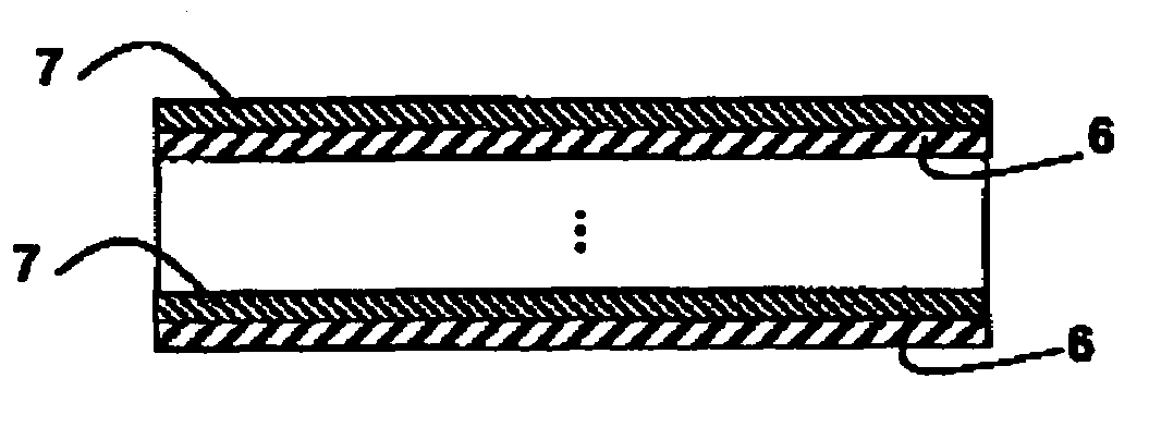
[0027]An optical device reflecting a range of wavelengths comprised between 10 nm and 20 nm comprises alternate superposed first and second layers 6 and 7 (FIG. 6). The first layers 6 are made of metal and preferably molybdenum or of metallic compound and preferably molybdenum carbide. The second layers 7 are formed by an amorphous silicon compound chosen from a-Si—Hx, a-Si—CHx, a-Si—Cx, a-Si—OHx, a-Si—Fx, a-Si—FHx, a-Si—Nx, and a-Si—NHx, x being comprised between 0.01 and 0.3. Thus a radical chosen from —H, —CH, —C, —OH, —F, —FH, —N and —NH is incorporated in the amorphous silicon so as to saturate the dangling bonds in the amorphous silicon. For example, what is meant by a-Si—Hx compound is a compound formed by hydrogenated amorphous silicon, i.e., amorphous silicon in which a predetermined hydrogen content is incorporated. The hydrogen content to be incorporated is situated in the range 1 to 25% of bonded atomic hydrogen.

[0028]The use of the second amorphous silicon compound laye...


PUM

PropertyMeasurementUnit
wavelengthsaaaaaaaaaa
thicknessaaaaaaaaaa

Abstract

An optical device reflecting a range of wavelengths comprised between 10 nm and 20 nm comprises alternate superposed first and second layers. The first layers are made of metal or metallic compound and the second layers are formed by an amorphous silicon compound chosen from a-Si—Hx, a-Si—CHx, a-Si—Cx, a-Si—OHx, a-Si—Fx, a-Si—FHx, a-Si—Nx, a-Si—NHx, x being comprised between 0.01 and 0.3. The use of second layers of amorphous silicon compound enables the mechanical stresses of the optical device to be stabilized up to at least 200° C. The optical device is preferably used as reflector for a lithography mask in the extreme ultraviolet (EUV).

Description

BACKGROUND OF THE INVENTION[0001]The invention relates to an optical device reflecting a range of wavelengths comprised between 10 nm and 20 nm and comprising alternate superposed first and second layers, said first layers being made of metal or metallic compound and said second layers comprising amorphous silicon.[0002]The invention also relates to a lithography mask comprising such an optical device.STATE OF THE ART[0003]Optical devices designed to reflect a range of wavelengths comprised in the extreme ultraviolet (EUV), i.e. between 10 nm and 20 nm, are generally composed of several alternate layers of molybdenum and silicon. Thus, the article “The hydrogenated amorphous silicon / nanodisperse metal (SIMAL) system—Films of unique electronic properties” (T.P. Drüsedau et al, Journal of Non Crystalline Solids 198–200 (1996), pages 829–832) mentions that multilayer systems comprising amorphous silicon or hydrogenated amorphous silicon and metals are used as mirrors in the field of so...

Claims


Application Information

Patent Timeline
Patent Type & Authority Patents(United States)
IPC IPC(8): G02B1/10G02B5/08G02B5/26G03F1/24G21K1/06H01L21/027
CPCB82Y10/00B82Y40/00G03F1/24G21K1/062G02B5/0891G21K2201/067
Inventor QUESNEL, ETIENNE
Owner COMMISSARIAT A LENERGIE ATOMIQUE ET AUX ENERGIES ALTERNATIVES
Why Eureka
Try Eureka