Method of manufacturing semiconductor device

a manufacturing method and semiconductor technology, applied in the direction of semiconductor devices, basic electric elements, electrical equipment, etc., can solve the problems of reducing the size of the device, reducing the isolation region, and reducing so as to reduce the junction leakage current, prevent the surface roughness of the semiconductor substrate, and reduce the effect of junction leakage curren

Inactive Publication Date: 2006-03-21
RENESAS TECH CORP
View PDF9 Cites 10 Cited by
  • Summary
  • Abstract
  • Description
  • Claims
  • Application Information

AI Technical Summary

Benefits of technology

[0031]An object of the present invention is to provide a method of manufacturing a semiconductor device which, by forming a protective oxide film, can prevent surface roughness of a semiconductor substrate and a gate electrode due to phosphoric acid and can achieve both reductions in junction leakage current (low power consumption) and improvements in the reliability of a gate oxide film (high reliability), without losing original advantages of a replacement sidewall process.
[0033]When the dummy sidewall and the impurity region are once formed and then the dummy sidewall is removed to extend the impurity region, the removal of the dummy sidewall is performed after formation of a protective film on the gate electrode and on the major surface of the impurity region or semiconductor substrate. This efficiently prevents conventional surface roughness of the upper surface of the gate electrode and the impurity region due to the removal of the dummy sidewall. By avoiding surface roughness of the semiconductor substrate and the gate electrode, both reductions in junction leakage current (low power consumption) and improvements in the reliability of the gate insulating film (high reliability) can be achieved without losing original advantages of the replacement sidewall process (e.g. suppression of short channel effect and improvements in drive capability).
[0035]Since heat of protective oxidation is not applied to the impurity region introduced by impurity implantation and also impurities in the impurity region and the gate electrode are activated in a later step, compatibility between suppression of impurity diffusion and an increase in the rate of activation can be increased with ease. By in this way, preventing excess impurity diffusion in, for example, the source and drain regions, it is possible to prevent a reduction in threshold voltage and an increase in variation of threshold voltage due to a deterioration in short channel characteristics and excess impurity diffusion in the gate electrode (caused by surface roughness of the gate insulating film due to gate impurities).
[0037]Since, by executing the step (g), the protective oxide film of a predetermined film thickness can be formed in short time in the step (d), excess impurity diffusion in the impurity region and in the gate electrode can be suppressed. By in this way, preventing excess impurity diffusion in, for example, the source and drain regions, it is possible to prevent a reduction in threshold voltage and an increase in variation of threshold voltage due to a deterioration in short channel characteristics and excess impurity diffusion in the gate electrode (caused by surface roughness of the gate insulating film due to gate impurities). Besides, channel impurity diffusion can also be suppressed, which makes it easy to form an advanced channel structure.

Problems solved by technology

Improvements in both short channel characteristics and drive capability of MOSFETs are becoming increasingly difficult as device dimensions shrink.
This is because, in the case of a SiO2 single-layer structure, an isolation oxide film also is etched at the time of removal of a sidewall, which arouses concern that an isolation region might recede significantly and thereby junction leakage properties might be worsened.
A sidewall of the SiN / SiO2 multilayer structure has another problem in that Si-exposed source / drain and gate have surface roughness, which is schematically illustrated with triangles in FIGS. 39 to 41.

Method used


Image

  • Method of manufacturing semiconductor device
  • Method of manufacturing semiconductor device
  • Method of manufacturing semiconductor device

Examples


second preferred embodiment

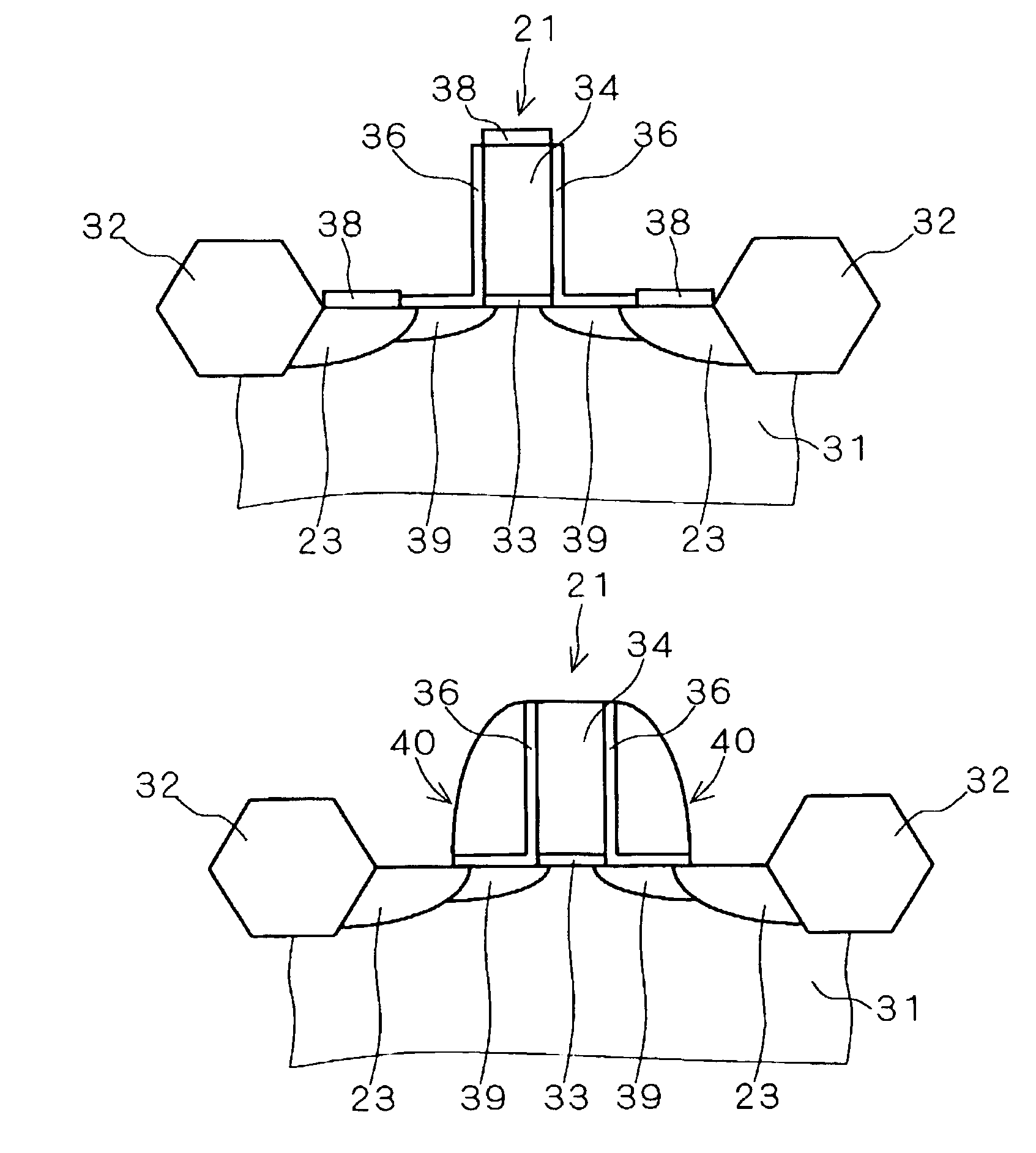
[0118]FIGS. 9 to 16 are schematic diagrams illustrating a process sequence of a semiconductor device manufacturing method according to a second preferred embodiment of the present invention. In FIGS. 9 to 16, components having functions similar to those of the first preferred embodiment are denoted by the same reference numerals. The semiconductor device manufacturing method according to this preferred embodiment changes the order of executing the source and drain (impurity region) formation process and the protective oxidation process.

[0119]

[0120]FIG. 9 shows a cross-section after completion of an element isolation process. As in the first preferred embodiment, the isolation oxide film 32 is formed for element isolation on the major surface of the semiconductor substrate 31. The isolation oxide film 32 sections an element region of the semiconductor substrate 31.

[0121]

[0122]As in the first preferred embodiment, the gate insulating film 33 (cf. FIG. 10) having a thickness of 0.5 to ...

third preferred embodiment

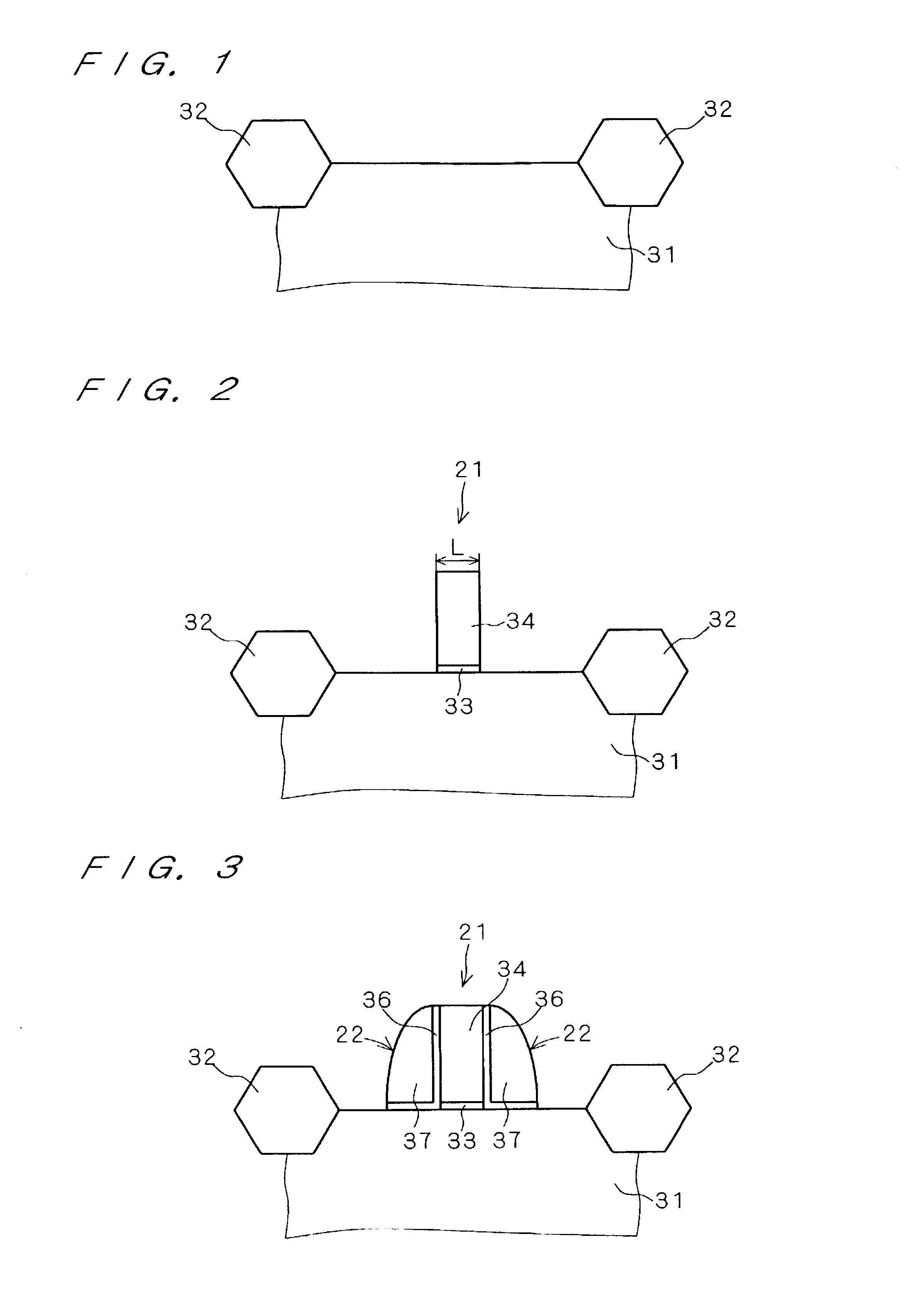
[0148]FIGS. 17 to 25 are schematic diagrams illustrating a process sequence of a semiconductor device manufacturing method according to a third preferred embodiment of the present invention. In FIGS. 17 to 25, components having functions similar to those of the first and second preferred embodiments are denoted by the same reference numerals. The semiconductor device manufacturing method according to this preferred embodiment differs from the first preferred embodiment in that impurity implantation for acceleration of oxidation is performed prior to protective oxidation. The details of the manufacturing method will be described hereinbelow.

[0149]

[0150]FIG. 17 shows a cross-section after completion of an element isolation process. As in the first preferred embodiment, the isolation oxide film 32 is formed for element isolation on the major surface of the semiconductor substrate 31.

[0151]

[0152]As in the first preferred embodiment, the gate insulating film 33 (cf. FIG. 18) having a thi...

fourth preferred embodiment

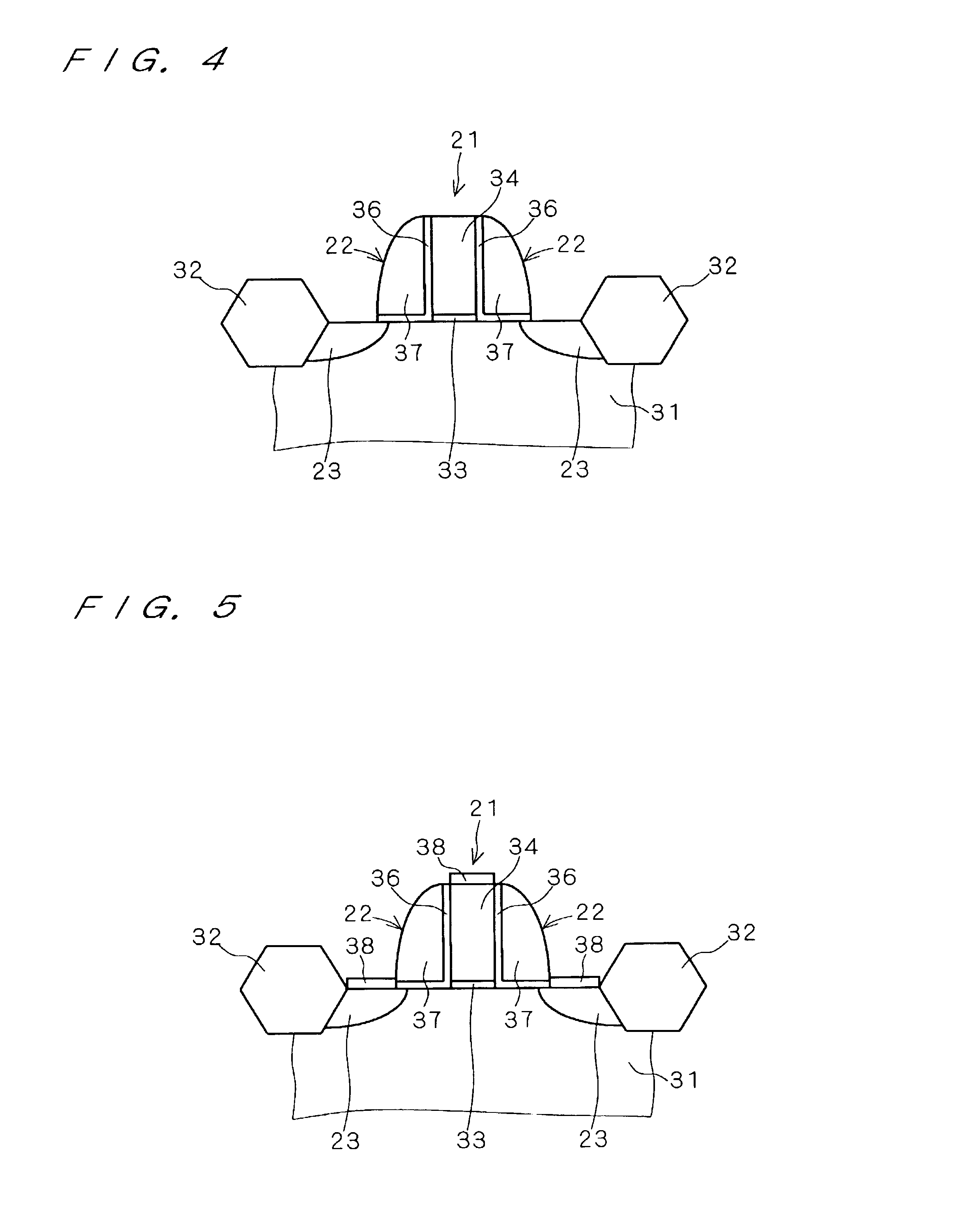
[0181]FIGS. 26 to 34 are schematic diagrams illustrating a process sequence of a semiconductor device manufacturing method according to a third preferred embodiment of the present invention. In FIGS. 26 to 34, components having functions similar to those of the first through third preferred embodiments are denoted by the same reference numerals. The semiconductor device manufacturing method according to this preferred embodiment differs from the first through third preferred embodiments in that the source and drain are raised. The details of the manufacturing method will be described hereinbelow.

[0182]

[0183]FIG. 26 shows a cross-section after completion of an element isolation process. As in the first preferred embodiment, the isolation oxide film 32 is formed for element isolation on the major surface of the semiconductor substrate 31.

[0184]

[0185]As in the first preferred embodiment, the gate insulating film 33 (cf. FIG. 27) having a thickness of 0.5 to 9 nm is formed on the major ...


PUM


Abstract

When a dummy sidewall and source and drain regions are once formed and then the dummy sidewall is removed to extend the source and drain regions, the removal of the dummy sidewall is performed after formation of a protective oxide film on a gate electrode and on the major surfaces of the source and drain regions. This efficiently prevents conventional surface roughness of the upper surface of the gate electrode and the impurity region due to the removal of the dummy sidewall.

Description

BACKGROUND OF THE INVENTION[0001]1. Field of the Invention[0002]The present invention relates to a method of manufacturing a semiconductor device having an MIS (Metal-Insulator-Semiconductor) structure.[0003]2. Description of the Background Art[0004]Improvements in both short channel characteristics and drive capability of MOSFETs are becoming increasingly difficult as device dimensions shrink. As a method to resolve this problem, a replacement sidewall technique has been suggested (in, for example, Japanese Patent Application Laid-open No. 2000-168323). The replacement sidewall technique is a technique for removing a sidewall after deep source / drain (deep S / D) implantation and activation annealing and then performing extension implantation and activation annealing for extension. This technique aims to resolve the problem of a conventional process that heat required for activation of deep S / D is applied also to extensions, and to satisfy both shallow junctions and low parasitic resi...

Claims


Application Information

Patent Timeline
Patent Type & Authority Patents(United States)
IPC IPC(8): H01L21/336H01L29/78
CPCH01L29/41783H01L29/6653H01L29/665H01L29/66492H01L21/18
Inventor SUGIHARA, KOHEISAYAMA, HIROKAZU
Owner RENESAS TECH CORP
Why Eureka
Try Eureka