Simplified dual damascene process

a damascene and process technology, applied in the direction of basic electric elements, semiconductor/solid-state device manufacturing, electric apparatus, etc., can solve the problems of poor isolation of the dielectric layer, the step of patterning the copper interconnect is not easily performed using the current etching technology, etc., and achieves the effect of low capacitance dielectric layer and less processing tim

Inactive Publication Date: 2006-03-21
GRACE SEMICON MFG CORP
View PDF4 Cites 6 Cited by
  • Summary
  • Abstract
  • Description
  • Claims
  • Application Information

AI Technical Summary

Benefits of technology

[0009]The present invention provides a simplified dual damascene process, in which the steps of the dielectric layer, the etch stop layer, and the stack dielectric layer in the conventional process are omitted.Additionally, the structure has a low dielectric constant intermetal dielectric (IMD) with a good trench profile.
[0010]The present invention also provides a simplified dual damascene process, which requires less processing time And has a low capacitance dielectric layer.

Problems solved by technology

When copper is used as the material of the interconnects, the step of patterning the copper interconnects is not easily performed using the current etching technology because the steam pressure of a halide of copper is not high enough.
Also, the capacitance of the dielectric layer increases, resulting in poor isolation of the dielectric layer.

Method used


Image

  • Simplified dual damascene process
  • Simplified dual damascene process
  • Simplified dual damascene process

Examples


Embodiment Construction

[0017]The present invention provides a simplified dual damascene process without the steps of the dielectric layer, the etch stopping layer, and the stack dielectric layer of the conventional process. The structure has an inter-metal dielectric (IMD) with low dielectric constant with a high selective ratio of organic layer versus dielectric layer to form a better trench structure.

[0018]Refer to FIGS. 3a through 3h, which are sectional diagrams illustrating the structure of each step according to an embodiment of the present invention.

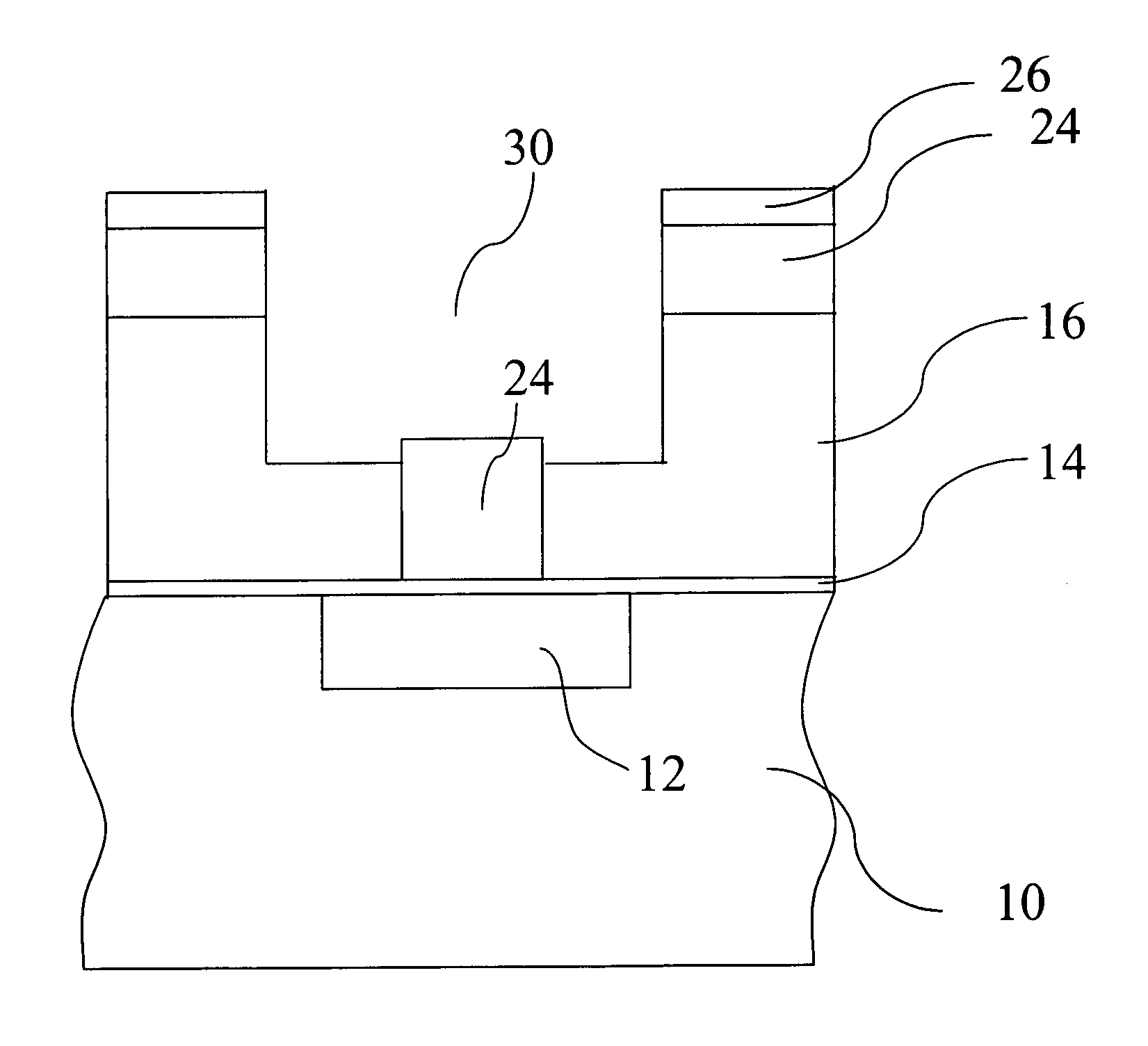
[0019]As shown in FIG. 3a, the semiconductor substrate 10 comprises MOS devices formed thereon. A layer of copper, a first metal layer 12, is deposited on the semiconductor substrate 10 by chemical deposition. A nitride stop layer 14 is deposited on the first metal layer 12. A dielectric layer 16 is then deposited on the nitride stop layer 14 using physical vapor deposition (PVD) or chemical vapor deposition (CVD). The material of the dielectric layer 1...


PUM


Abstract

A simplified dual damascene process is disclosed. In the dual damascene process, a semiconductor substrate with MOS devices having a first metal layer, an etch stopping layer, and a dielectric layer in sequence are formed thereon. A via is formed on the dielectric layer by lithography. An organic layer is then formed. A trench is formed on the dielectric layer by the organic layer, thereby forming a dual damascene structure comprised of the trench and the via. The present invention is directed to a simplified dual damascene process, which can obtain a better trench profile without increasing the dielectric constant of the inter-metal dielectric (IMD).

Description

BACKGROUND OF THE INVENTION[0001]1. Field of the Invention[0002]The present invention relates to a dual damascene process, in particular, to a simplified dual damascene process, in which the steps of stacking the dielectric layer, the etch stop layer, and the stack dielectric layer in the conventional process are omitted and the dielectric constant of the inter-metal dielectric (IMD) is reduced, thereby obtaining a simplified dual damascene process with good trench profile.[0003]2. Description of the Prior Art[0004]As the lines of IC design in semiconductor processing become more and more highly concentrated, the unit area bears a larger and larger current. Since copper has both a low resistance and a high anti-electromigration resistance ability, conventional aluminum interconnect processing is substituted with copper interconnect processing.[0005]When copper is used as the material of the interconnects, the step of patterning the copper interconnects is not easily performed using ...

Claims


Application Information

Patent Timeline
Patent Type & Authority Patents(United States)
IPC IPC(8): H01L21/302H01L21/3205H01L21/4763H01L21/768
CPCH01L21/76808
Inventor WOO, BEEN JON
Owner GRACE SEMICON MFG CORP
Why Eureka
Try Eureka