

NMOS composite device Vds bootstrappers
a composite device and nmos technology, applied in the field of cmos analog circuits and cmos analog circuit design, can solve the problems of derogatory effects on linearity, increase of 1/f noise and channel length modulation, and decrease of the effective output resistance of the devi
- Summary
- Abstract
- Description
- Claims
- Application Information
AI Technical Summary
Benefits of technology
Problems solved by technology
Method used
Image

Examples
Embodiment Construction
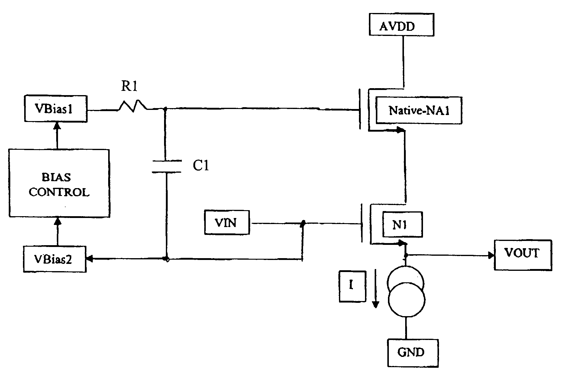
[0011]The present invention seeks to mitigate the effects of decreased power supply rejection and increased channel length modulation in minimum or short channel length devices by using a device commonly available in advanced analog CMOS process technology called a ‘Native’ NMOS device, or alternatively, a low threshold NMOS device. The ‘Native’ device or ‘0 Vt’ device (0V threshold voltage) is typically formed in the substrate without the use of a channel implant to alter the threshold voltage and / or to improve source-drain punch through. The benefits of the Native device are its near 0V threshold voltage that enables circuit operation under low supply voltages and with less overdrive than a standard minimum channel length device.
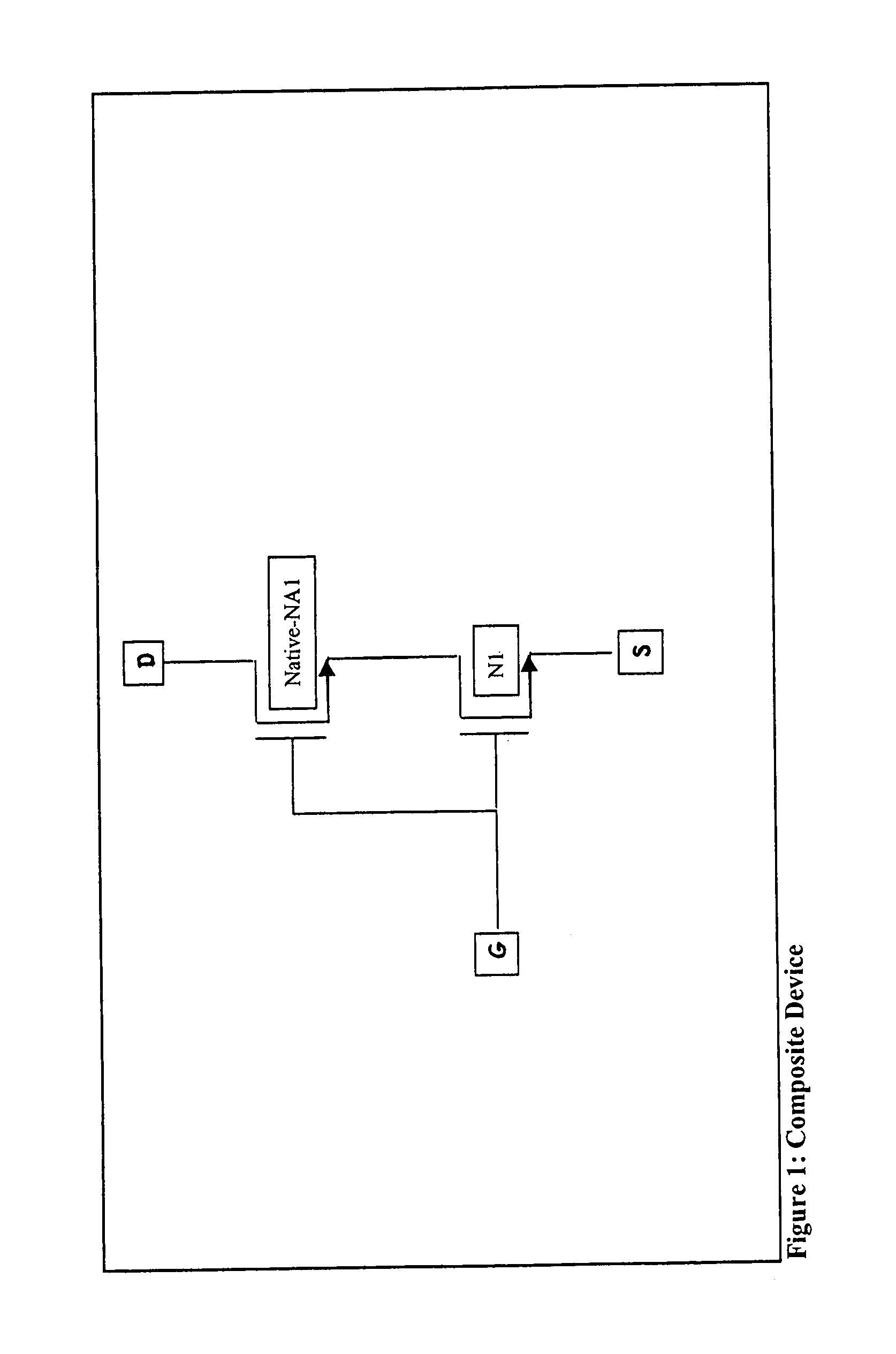
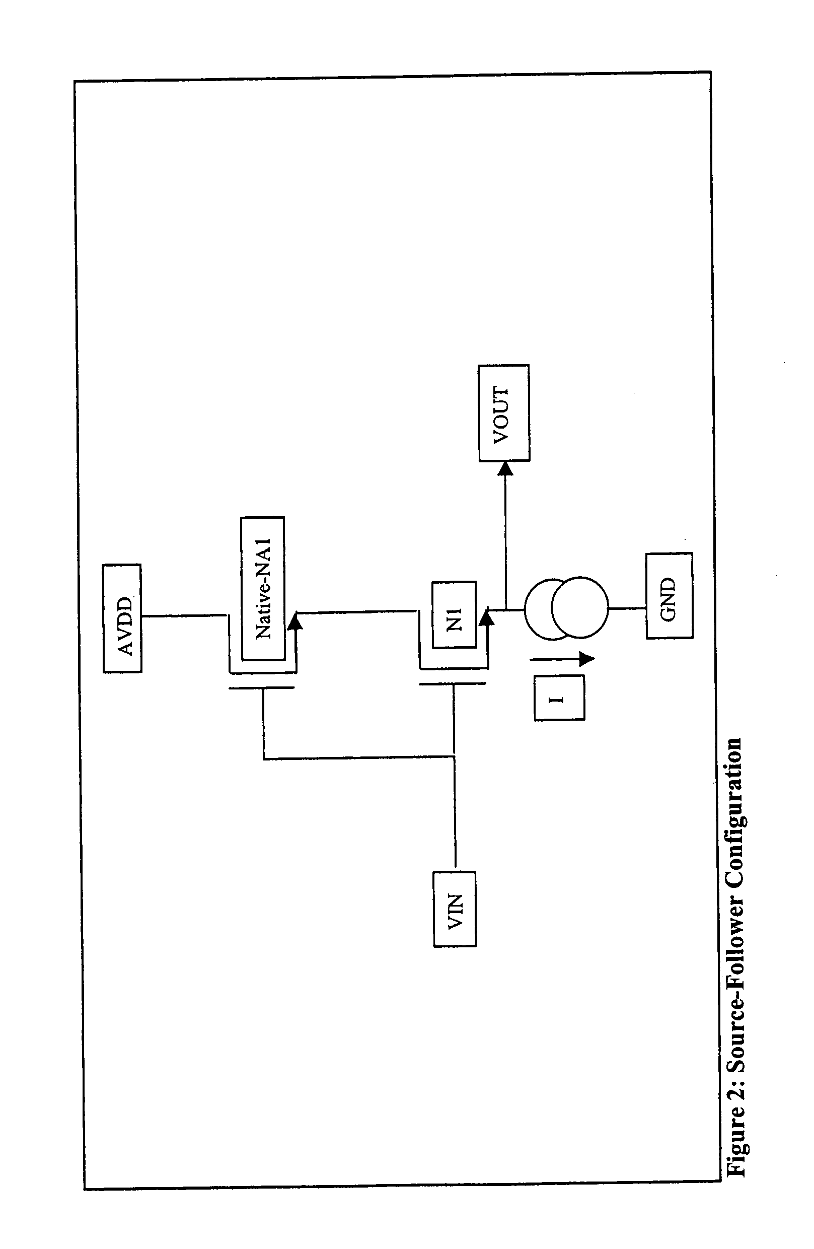
[0012]One embodiment of this invention (FIG. 1) uses a NMOS device N1 with a Native NMOS device NA1 stacked thereon, the two devices having a common gate connection to form a three terminal composite device having a source (S) connection, a drain (D) conne...
PUM
 Abstract
Description
Claims
Application Information