Charge pump circuit incorporating corresponding parallel charge pump stages and method therefor

a charge pump and parallel charge pump technology, applied in the field of capacitor voltage multiplier circuits, can solve the problems of significant power loss, significant amount of power, and significant loss of diodes lost by each charge pump stage, and achieve the effect of increasing the current that must be supplied by the user, significant amount of power, and significant power loss

Inactive Publication Date: 2006-04-04
INNOVATIVE MEMORY SYST INC
View PDF23 Cites 155 Cited by
  • Summary
  • Abstract
  • Description
  • Claims
  • Application Information

AI Technical Summary

Benefits of technology

[0013]The present invention provides an improved charge pump circuit which, in certain embodiments, efficiently utilizes multiple charge pump stages to produce output voltages much larger t

Problems solved by technology

At lower power supply voltages, the diode drop lost by each charge pump stage significantly affects the final output voltage achievable by such a charge pump circuit.
Moreover, such voltage generator circuits also may consume a significant amount of power relative to the remainder of the circuit, and thus increase the current that must be supplied by the user (e.g., by the VDD power supply).
Any increase in power dissipation may also increase the temperature of the die during operation.
In a battery-powered environment, any increase in power consumed by a device may have significant implications for battery life, and any additional heat generated may also be difficult to dissipate.
An N-channel transistor (e.g., NMOS) device may have a smaller forward drop than either a P-channel transistor (e.g., PMOS) device or a diode, but an

Method used


Image

  • Charge pump circuit incorporating corresponding parallel charge pump stages and method therefor
  • Charge pump circuit incorporating corresponding parallel charge pump stages and method therefor
  • Charge pump circuit incorporating corresponding parallel charge pump stages and method therefor

Examples


Embodiment Construction

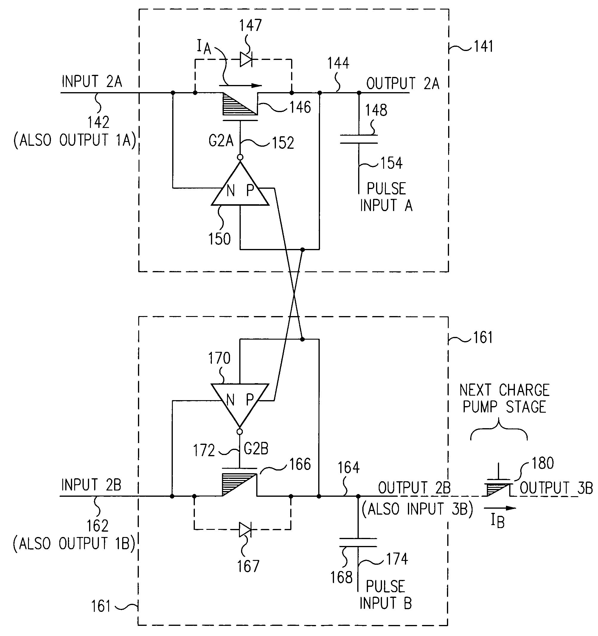
[0037]Referring now to FIG. 3, two charge pump stages 141, 161 within an exemplary charge pump circuit 140 are depicted. Charge pump stage 141 represents a charge pump stage within a first string of series-coupled charge pump stages, while charge pump stage 161 represents a charge pump stage within a second string of series-coupled (i.e., serially-connected) charge pump stages. The charge pump stage 141 within the first string corresponds to the charge pump stage 161 in the other string, and is controlled by a node in the corresponding charge pump stage 161.

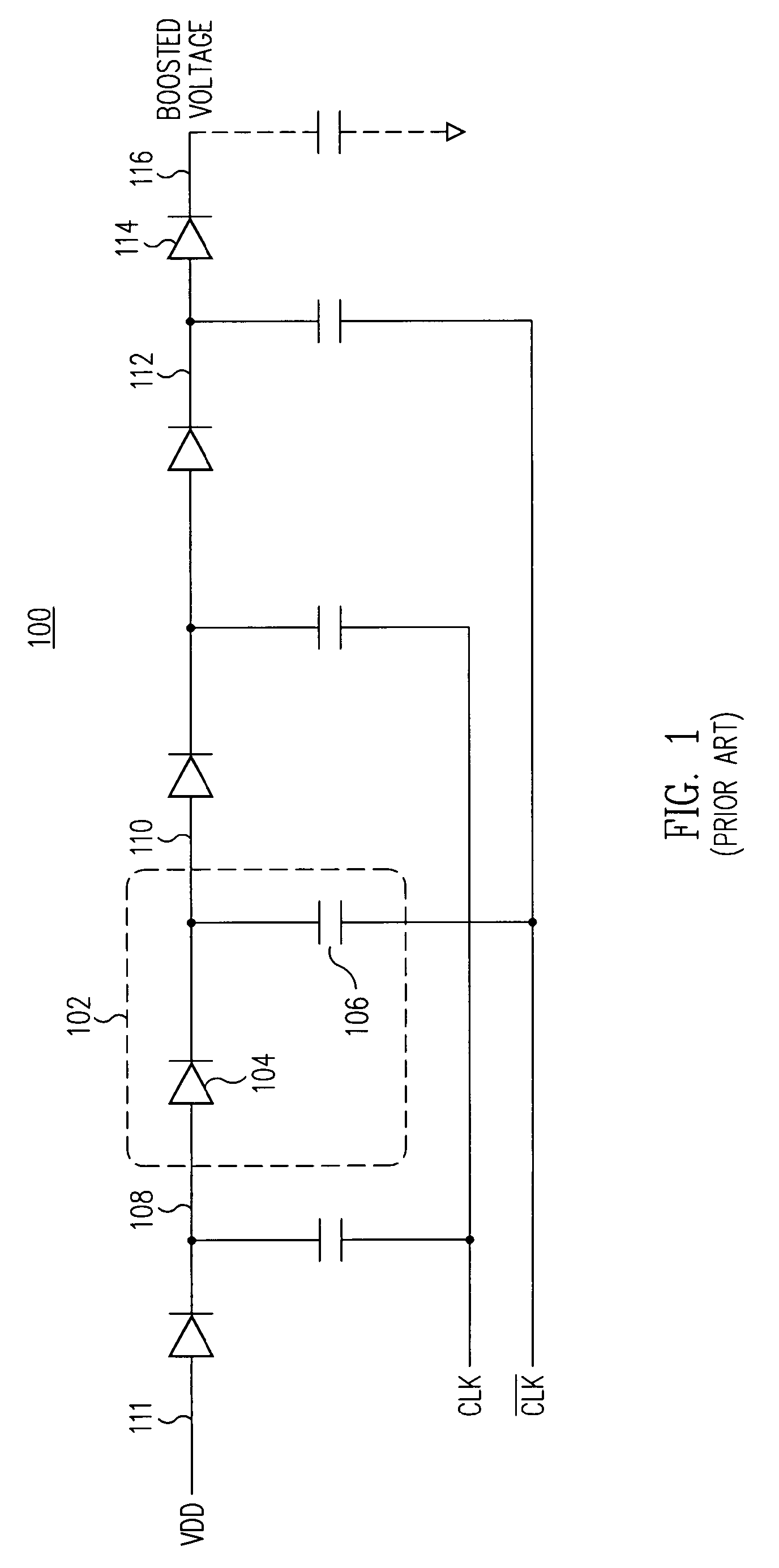
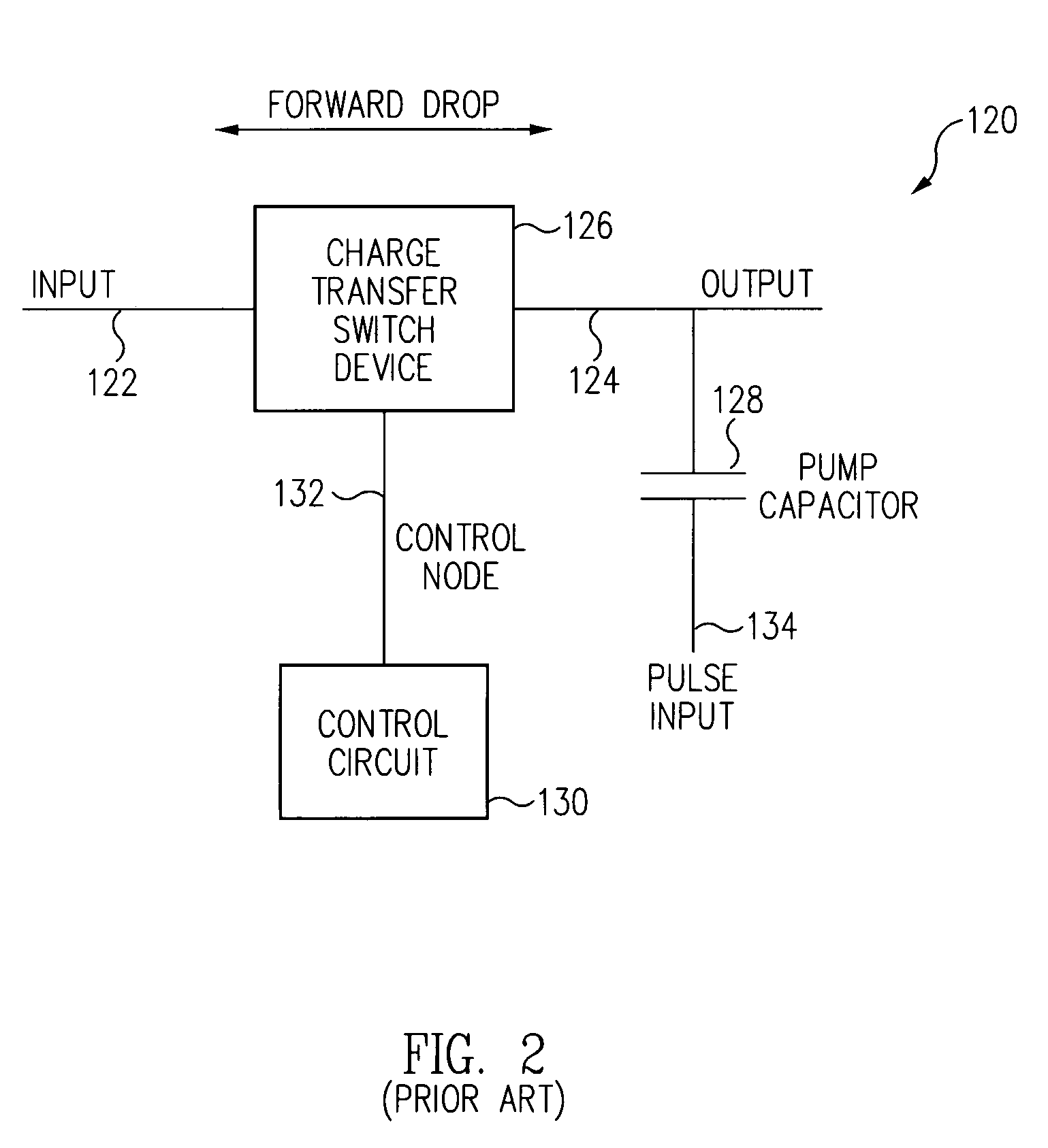
[0038]The charge pump stage 141 includes a charge transfer switch 146 connecting an input 142 to an output 144, a pump capacitor 148 connected to the output 144, and a control circuit 150 for generating a control node 152 for the charge transfer switch 146. A pulse input 154 is driven by a pulse signal, such as one of a complementary pair of clock signals CLK and / CLK, depending upon the placement of the charge pump stage within ...


PUM


Abstract

An improved charge pump circuit efficiently utilizes multiple charge pump stages to produce output voltages much larger than the power supply voltage by incorporating, in some embodiments, two parallel strings of series-coupled charge pump stages. Each corresponding charge pump stage in one string is controlled at least by a node in the corresponding charge pump stage of the other string.

Description

BACKGROUND[0001]1. Field of the Invention[0002]The present invention relates to semiconductor voltage generator circuits, and particularly to capacitive voltage multiplier circuits.[0003]2. Description of the Related Art[0004]Many integrated circuits, particularly those using a single power supply voltage, incorporate on-chip circuitry to generate a “boosted” voltage having a magnitude greater than the power supply voltage. Frequently this boosted voltage is used as a veritable power supply voltage for portions of the circuitry contained on the integrated circuit. For example, certain types of semiconductor memories, such as “flash” EEPROM memories, write a memory cell by accelerating electrons across a tunneling dielectric and storing the charge on a floating gate above a field effect transistor. On contemporary devices, this acceleration of charge across the tunneling dielectric frequently requires a “write voltage” on the order of 8 volts, yet the remainder of the operations of t...

Claims


Application Information

Patent Timeline
IPC IPC(8): G05F1/10G05F3/02H02M3/07
CPCH02M3/073H02M2003/077H02M3/077
Inventor THORP, TYLER J.SCHEUERLEIN, ROY E.
Owner INNOVATIVE MEMORY SYST INC
Why Eureka
Try Eureka