Semiconductor device having external contact terminals and method for using the same

a technology of contact terminals and semiconductor devices, which is applied in the direction of individual semiconductor device testing, coupling device connection, instruments, etc., can solve the problems of increasing electric contact resistance, inaccurate transmission of test signals, and difficulty in completely removing dirt once adhered

Inactive Publication Date: 2006-04-11
SHINKO ELECTRIC IND CO LTD
View PDF23 Cites 69 Cited by
  • Summary
  • Abstract
  • Description
  • Claims
  • Application Information

AI Technical Summary

Benefits of technology

[0008]The present invention has been made under such the circumstance, and the problem to be solved is to provide a semiconductor device having a number of springy external contact pins or terminals of a micro-spring system, usable for a long period free from the variation of a contact voltage of the respective contact pin or terminal even if it has repeated the contact several hundreds or thousands times, and a method for using the semiconductor device.

Problems solved by technology

In such a semiconductor device, while the contact terminals repeat making contact with pads or solder balls on an interposer or a connector board several hundreds or thousands times, a surface of the terminal may be become contaminated or adhered with dirt or solder transferred from the mating object, which increases the electric contact resistance of the external terminal, causing a problem particularly in a high-frequency probe pin in that a test signal is not accurately transmitted even if the adhered solder is slight in amount.
However, even though the rinsing is carried out, it is difficult to completely remove the dirt which has been once adhered.
Accordingly, there is a problem in that the contact resistance is difficult to maintain at a low level in a stable manner for a long period, which means that the device is not durable against a long term use in a stable state.
In addition, as the semiconductor device or the like is generally expensive, it is not economical to frequently replace it with a new one.
However, a method has not yet been found by which the external pin could be used in a stable state for a long period even if the contact is repeated several hundreds or thousands times.

Method used


Image

  • Semiconductor device having external contact terminals and method for using the same
  • Semiconductor device having external contact terminals and method for using the same
  • Semiconductor device having external contact terminals and method for using the same

Examples


Embodiment Construction

[0025]Embodiments of the present invention will be described in detail, below, with reference to the attached drawings.

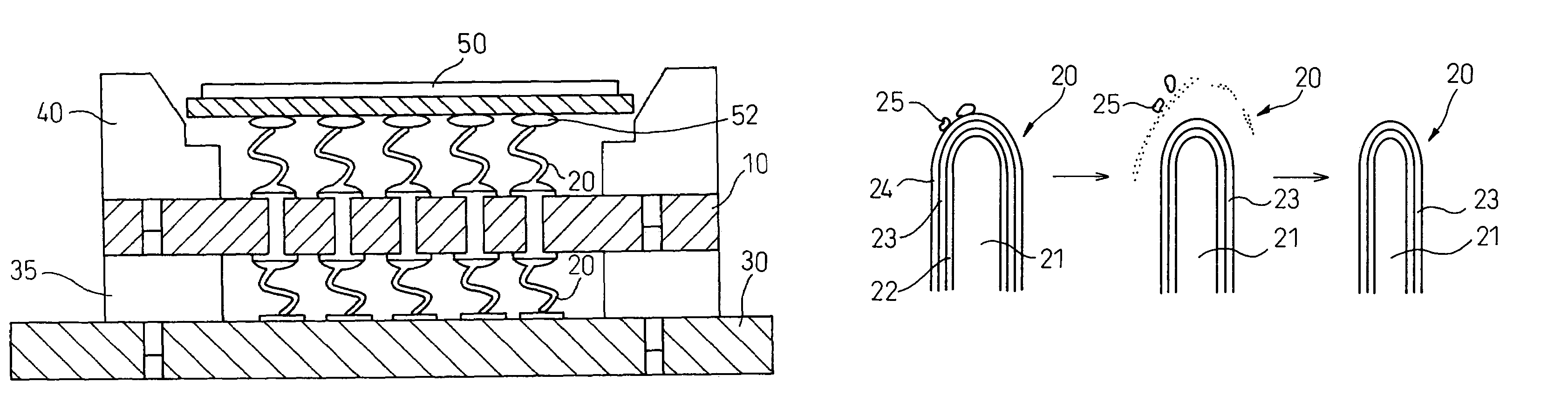
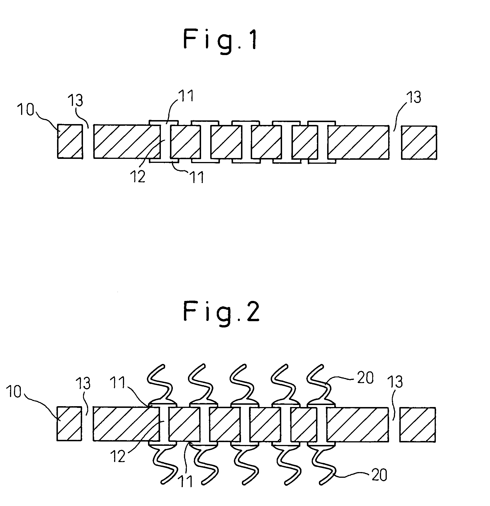
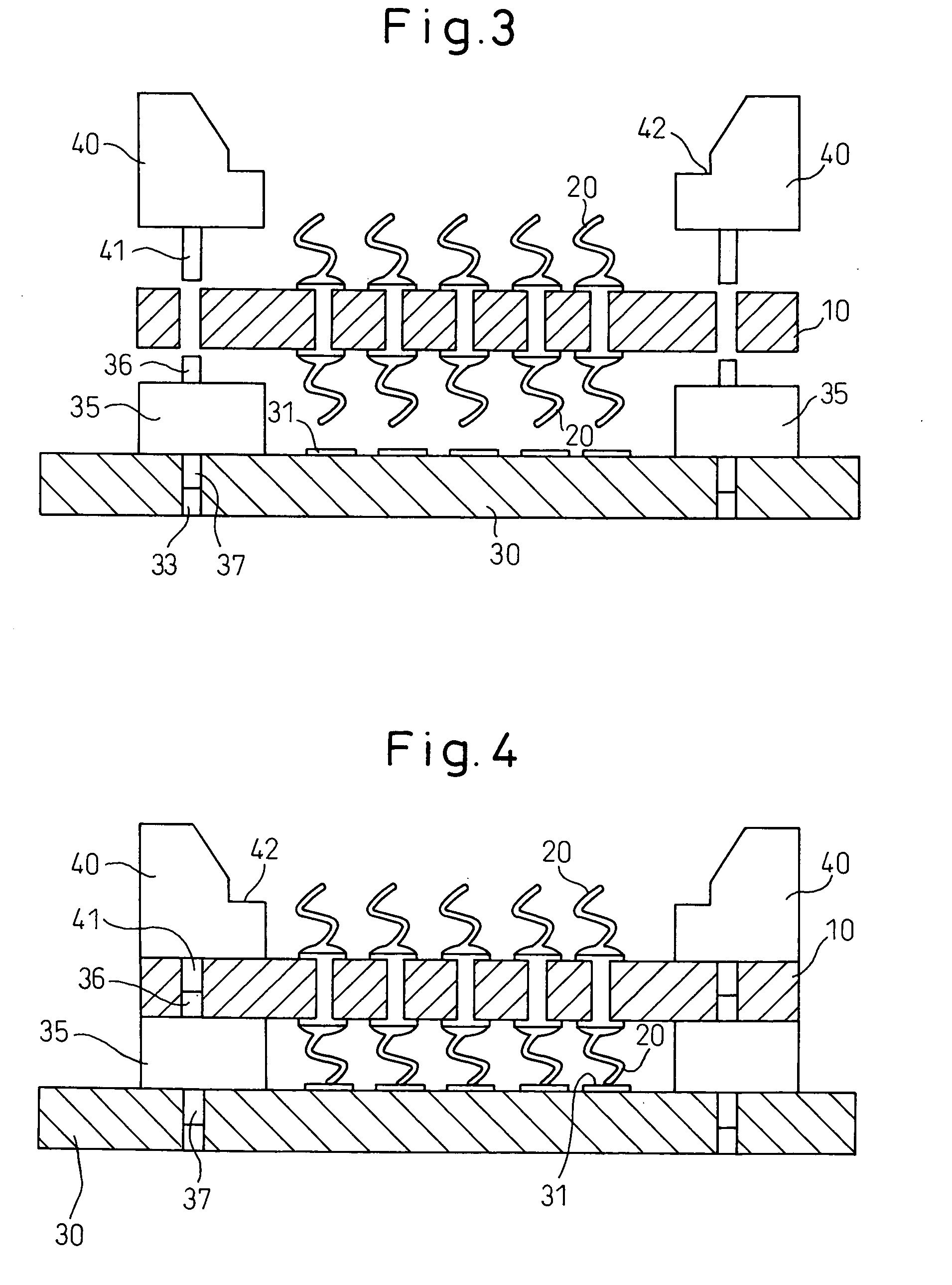
[0026]FIGS. 1 to 4 illustrate a series of processes for producing the inventive semiconductor device having external contact terminals. First, in FIG. 1, a support board 10 is prepared, in which conductor pads 11 and wirings 12 are provided for forming micro-springs (external contact pins of terminals). This support board 10 may be any of various boards generally used as a board for a semiconductor device, such as a glass-epoxy resin board or a ceramic board.

[0027]In general, a number of conductor pads 11 for forming the micro-springs are arranged both on front and back surfaces of the support board in the X direction and the Y direction at a pitch. The wirings 12 are connected to the conductor pads 11, respectively. There are through-hole wirings among the wirings 12, for connecting the conductor pads 11 respectively formed on the front and back surfaces of the sup...


PUM


Abstract

A method of using a semiconductor device having a plurality of external contact terminals formed of springy wires, usable in a stable state free from variation of contact voltage for a long period even if a contact terminal repeatedly makes contact several hundreds or thousands of times. A tip end of the external contact terminal is plated with individually, selectively removable multiple films, and the plated films are individually, selectively removed by an etching treatment, in accordance with the degree of contamination of the tip end of the external contact terminal, and then the external contact terminal is rinsed and rendered reusable.

Description

BACKGROUND OF THE INVENTION[0001]1. Field of the Invention[0002]The present invention relates to a semiconductor device having external contact terminals and a method for using the same and, particularty to a semiconductor device having external terminals, such as a semiconductor socket having a number of springy external contact pins or terminals of a micro-spring system, which are used while being brought into contact with pads or solder balls of an interposer or a connector board.[0003]2. Description of the Related Art[0004]In the prior art, in a semiconductor device having a number of springy external contact pins or terminals of a micro-spring type, used as a test probe or otherwise, the external contact pin or terminal is made, for example, of a gold (Au) wire for bonding, which surface is plated with palladium (Pd), indium (in) or others. In such a semiconductor device, while the contact terminals repeat making contact with pads or solder balls on an interposer or a connector...

Claims


Application Information

Patent Timeline
Patent Type & Authority Patents(United States)
IPC IPC(8): H01R12/00G01R31/26G01R1/073H01L23/32H01R13/03H01R13/24H01R13/33H01R33/76
CPCH01R13/2407H01R13/33H01R13/2435H01R13/03H01L2924/19107H01R2201/20H01L2224/16H01L2224/45144H01L2924/00
Inventor HIGASHI, MITSUTOSHI
Owner SHINKO ELECTRIC IND CO LTD
Why Eureka
Try Eureka