Method of attaching optical waveguide component to printed circuit board

a technology of optical waveguide and printed circuit board, which is applied in the direction of photomechanical treatment originals, instruments, photomechanical equipment, etc., can solve the problems of lowering the optical interfacing properties, difficult application to a multi-layer printed circuit board, and inevitably required optical interfacing medium, so as to improve the flatness and precise alignment of the optical waveguide componen

Inactive Publication Date: 2006-04-11
SAMSUNG ELECTRO MECHANICS CO LTD
View PDF2 Cites 8 Cited by
  • Summary
  • Abstract
  • Description
  • Claims
  • Application Information

AI Technical Summary

Benefits of technology

[0010]The present inventors have conducted extensive studies to avoid the above disadvantages, resulting in the finding that the optical waveguide component can be attached to the printed circuit board through the steps of pre-bonding and main-bonding with improved flatness and precise alignment of the optical waveguide component without chemical or thermal damage to the optical waveguide component upon attaching, by use of an adhesive tape (and / or by use of a groove formed on or in the printed circuit board), for receiving the optical waveguide component.
[0011]Therefore, an object of the present invention is to provide a method of attaching an optical waveguide component to a printed circuit board, which enables improved flatness and precise alignment of the optical waveguide component without chemical or thermal damage to the optical waveguide component upon attaching.

Problems solved by technology

However, the electric signal is subject to a restriction attributable to electro magnetic susceptibility (EMS) during a high speed switching within a giga band, and thus an optically interfacing medium is inevitably required.
However, this patent is disadvantageous in that the optical wiring layer is directly formed on the backside of the electrical wiring board, which makes the application to a multilayer printed circuit board difficult, and thus lowering optically interfacing properties.
Furthermore, since a polymer employable for an optical waveguide component is different from a material constituting the printed circuit board, the delamination and air voids may occur at an interface between the optical waveguide component and the printed circuit board.

Method used


Image

  • Method of attaching optical waveguide component to printed circuit board
  • Method of attaching optical waveguide component to printed circuit board
  • Method of attaching optical waveguide component to printed circuit board

Examples


Embodiment Construction

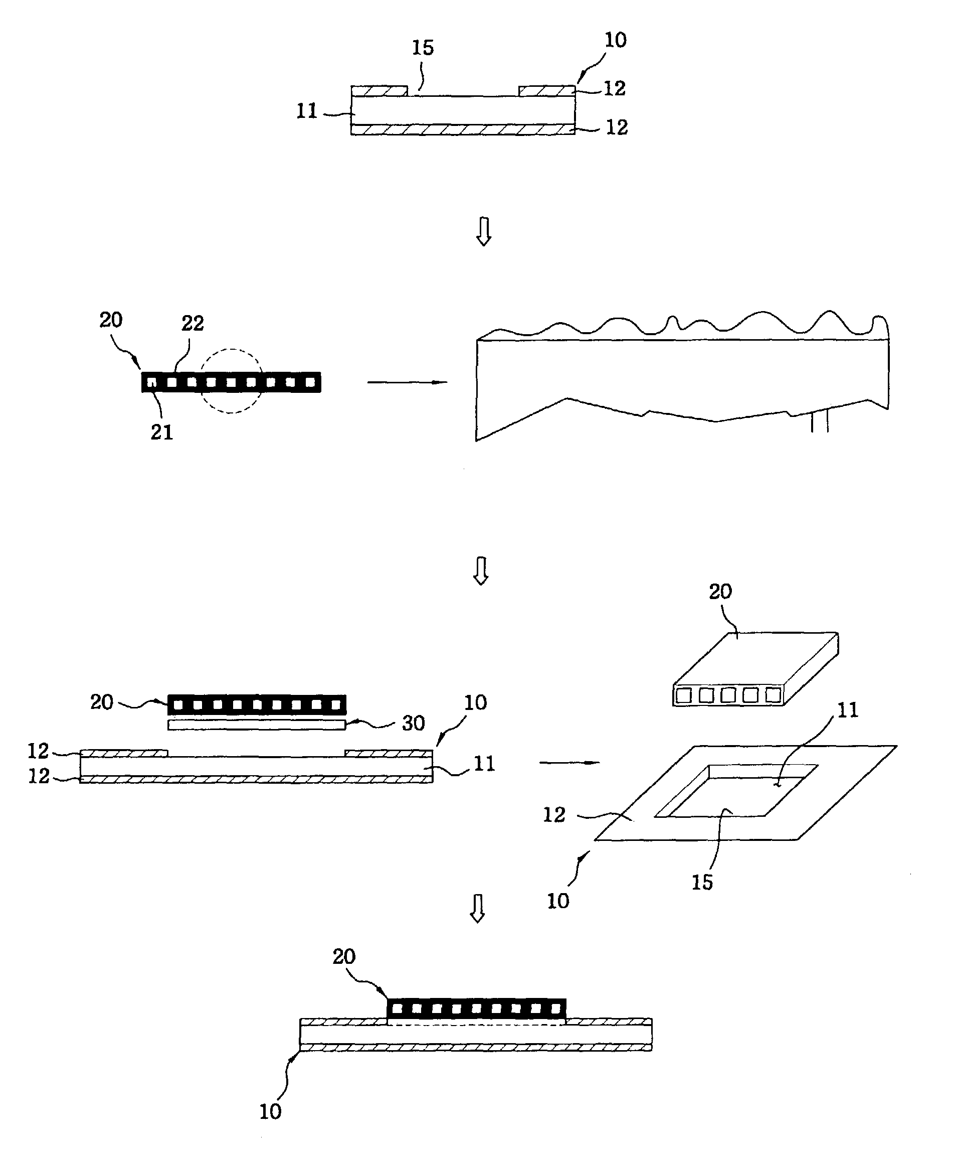
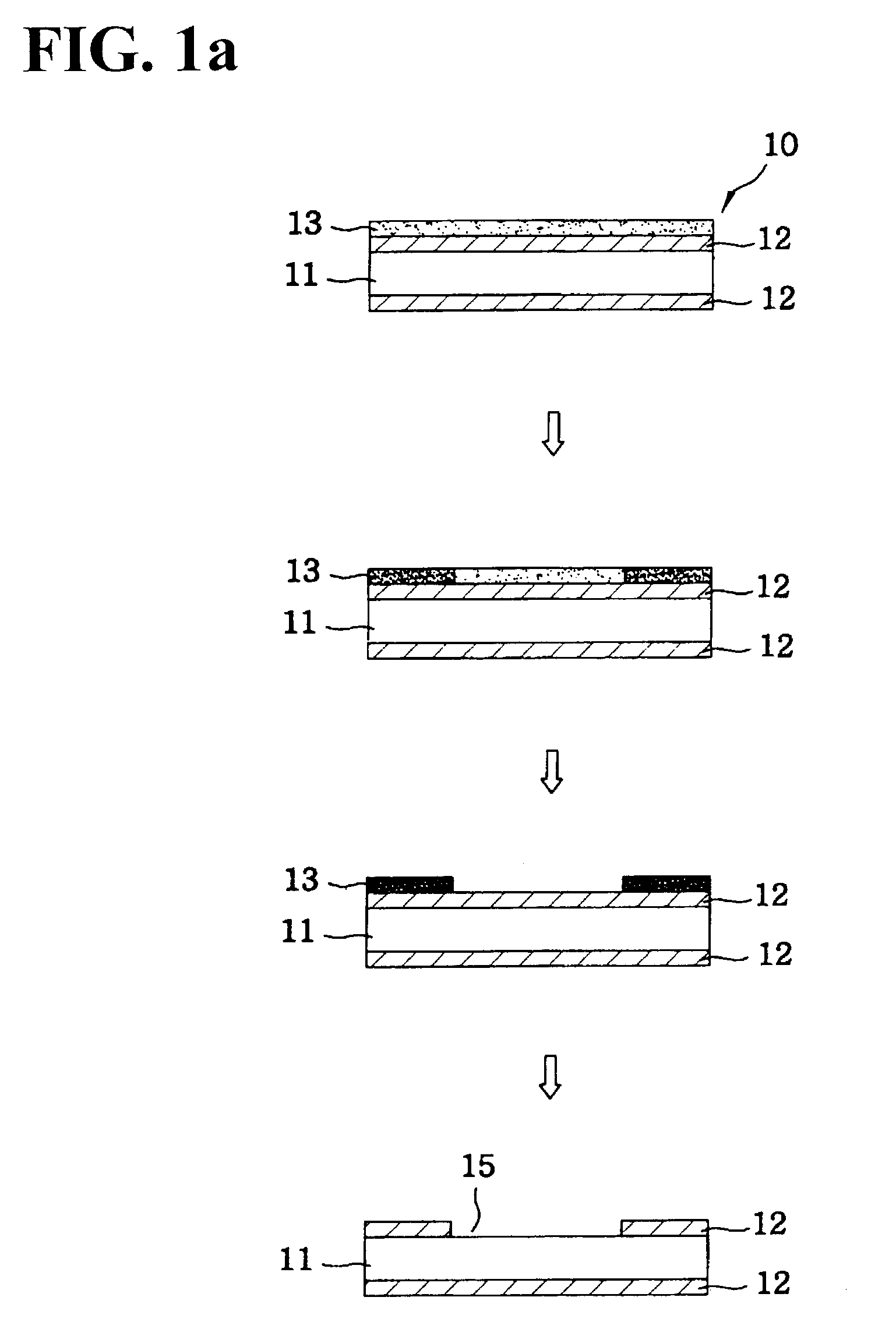
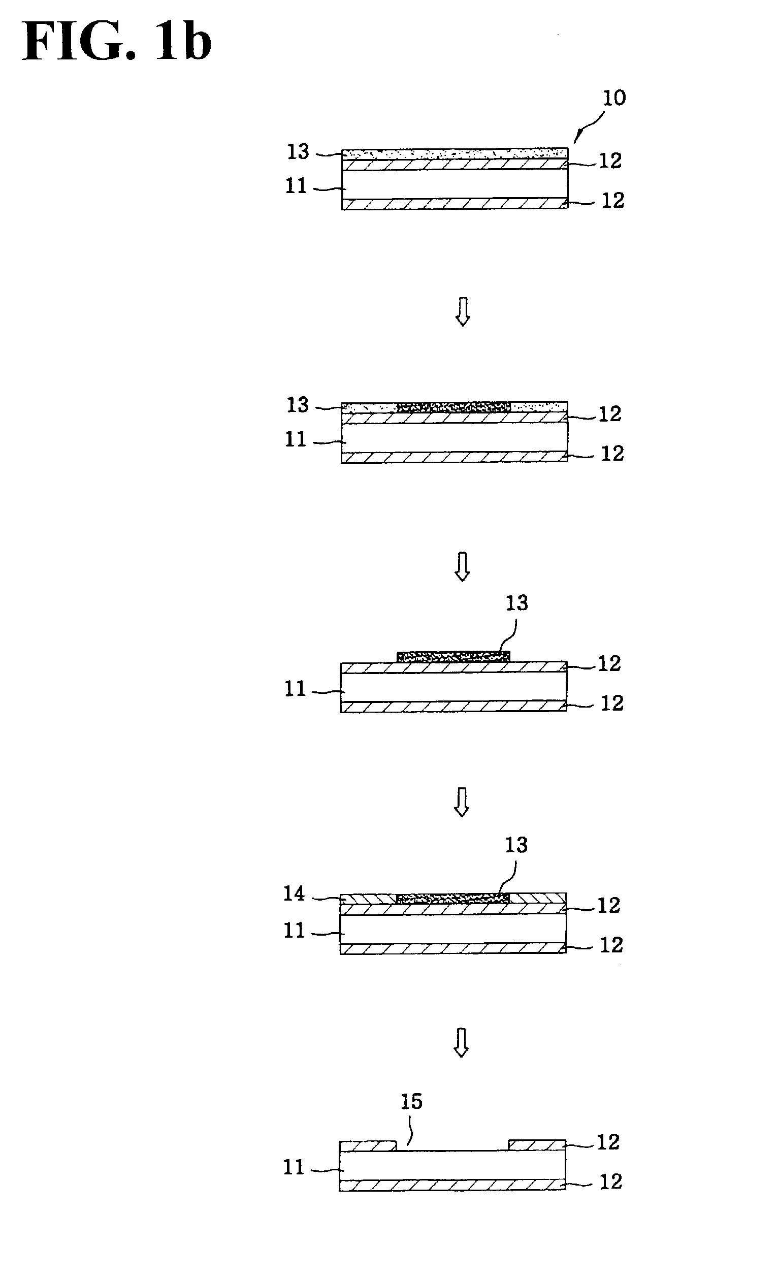
[0040]The present invention provides a method of attaching an optical waveguide component to a printed circuit board, which enables improved flatness and precise alignment of the optical waveguide component without chemical or thermal-damage to the optical waveguide-component upon attaching.

[0041]Examples of the printed circuit board employable in the present invention include a double-sided printed circuit board having one dielectric substrate layer and two circuit layers, and a multilayer printed circuit board consisting of plural dielectric layers and circuit layers. As such, the dielectric layer may be a dielectric substrate layer or a dielectric adhesive layer.

[0042]It is well known in the art that the dielectric adhesive layer is employed for laminating a plurality of layers constituting a multilayer printed circuit board. In general, film-typed dielectric adhesive, which is referred to as a prepreg, is widely used in such laminating procedures.

[0043]The circuit layer refers t...


PUM

PropertyMeasurementUnit
conductiveaaaaaaaaaa
thicknessaaaaaaaaaa
surface roughnessaaaaaaaaaa

Abstract

Disclosed is a method of attaching an optical waveguide component to a printed circuit board, which is a double-sided or a multilayer printed circuit board, through pre-bonding and main-bonding by use of an adhesive tape. Prior to being attached to the printed circuit board, the optical waveguide component is preferably subjected to a plasma surface treatment to give a surface roughness thereto. The present method is advantageous in that the optical waveguide component can be attached to the printed circuit board with improved flatness and precise alignment without causing chemical or thermal damage to the optical waveguide component.

Description

BACKGROUND OF THE INVENTION[0001]1. Field of the Invention[0002]The present invention relates to a method of attaching an optical waveguide component to a printed circuit board. More particularly, the present invention is directed to a method of attaching an optical waveguide component to a printed circuit board, which enables improved flatness and precise alignment of the optical waveguide component without chemical or thermal damage to the optical waveguide component upon attaching.[0003]2. Description of the Prior Art[0004]As well known to those skilled in the art, when components are electrically connected with each other, or power voltage or ground voltage is supplied in large-scaled devices such as a computer, an electric signal is conventionally applied through conductive copper patterns laminated on a printed circuit board to form at least one electric circuit on an inner and outer layer of the printed circuit board. Meanwhile, nowadays, there is a need for a broad bandwidth...

Claims


Application Information

Patent Timeline
Patent Type & Authority Patents(United States)
IPC IPC(8): B32B37/00G02B6/42G02B6/43H05K3/32H05K1/02
CPCH05K1/0274G02B6/423G02B6/4236G02B6/43Y10T156/109Y10T156/1062Y10T156/1064Y10T29/49126Y10T156/1082Y10T156/1304Y10T156/1309H05K3/32
Inventor KIM, YOUNG-WOOCHO, YOUNG-SANGYANG, DEK-GINYIM, KYU-HYOK
Owner SAMSUNG ELECTRO MECHANICS CO LTD
Why Eureka
Try Eureka