Interconnection for organic devices

a technology of interconnection and organic devices, applied in the direction of thermoelectric device junction materials, semiconductor devices, electrical apparatus, etc., can solve the problems of high risk of damage, low reliability, difficult processing, etc., and achieve the effect of improving the interconnection of devices and enhancing conductivity

Inactive Publication Date: 2006-04-11
PICTIVA DISPLAY INT LTD
View PDF19 Cites 23 Cited by
  • Summary
  • Abstract
  • Description
  • Claims
  • Application Information

AI Technical Summary

Benefits of technology

[0005]The invention relates to improved interconnection of devices, such as OLED devices. A bond pad region is provided, the bond pad region having bond pads comprising a conductive material that is stable when exposed to atmospheric constituents such as water and oxygen.

Problems solved by technology

However, the contact layer is exposed to the environment at portions such as 210, and is highly susceptible to damage caused by reaction with atmospheric components such as

Method used


Image

  • Interconnection for organic devices
  • Interconnection for organic devices
  • Interconnection for organic devices

Examples


Embodiment Construction

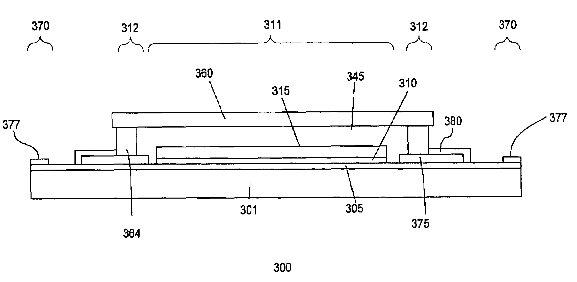
[0011]The invention relates to improved interconnection of devices. The interconnection results in devices which are more reliable and relatively inexpensive to produce. FIG. 3 shows a device 300 in accordance with one embodiment of the invention. In one embodiment, the device comprises a substrate 301 having an active region 311 defined thereon. The substrate comprises, for example, glass. Materials, such as silicon or other semiconductor materials, are also useful. To form flexible devices, materials such as plastics, can be used. Various other materials, which can provide sufficient mechanical stability for forming the device, are also useful.

[0012]The active region comprises one or more active components of the device. In one embodiment, the active region comprises one or more OLED cells. The active region may also comprise other types of electronic components. An OLED cell comprises one or more organic layers (polymer stack) 310 sandwiched between first and second electrodes (3...


PUM


Abstract

A device having bond pads within a bond pad region, the bond pads comprising a conductive material that is stable when exposed to atmospheric constituents. The bond pads can be formed from conductive oxide materials such as indium tin oxide. A contact layer is provided to enhance the conductivity between the bond pads and the active component of the device.

Description

BACKGROUND OF INVENTION[0001]OLED devices can serve as displays for various types of consumer electronic products, such as automobile stereo displays, cellular phones, cellular smart phones, personal organizers, pagers, advertising panels, touch screen displays, teleconferencing and multimedia products, virtual reality products and display kiosks. Referring to FIG. 1, a conventional OLED device 100 is shown. The OLED device comprises a functional stack formed on a substrate 101. The functional stack comprises one or more organic functional layers 102 between a transparent first conductive layer 104 (e.g., indium tin oxide or ITO) and a second conductive layer 106. The conductive layers serve as electrodes. OLED cells are located in the active region where the cathodes and anodes overlap. A cap 160 may be provided to hermetically seal the active components. A contact layer 150 can be formed over the first conductive layer, the contact layer extending to the exterior of the encapsulat...

Claims


Application Information

Patent Timeline
IPC IPC(8): H01L33/00H01L35/24H01L51/00H01L27/15H01L27/32H01L51/52
CPCH01L51/5237H01L27/3288H10K59/179H10K50/841H10K50/844H10K77/10H01L31/022475H01L21/56H01L2924/01013H01L2924/01079H01L2924/01047H01L2924/01029H01L2924/01024H01L2224/16012
Inventor GUENTHER, EWALDLIM, HOOI BINABDUL MANAF, SHAHROL IZZANNIEIGENBRODT, STEFANTENG, SOONG LIN
Owner PICTIVA DISPLAY INT LTD
Why Eureka
Try Eureka