Electrostatic discharge protection circuit with feedback enhanced triggering

a protection circuit and electrostatic discharge technology, applied in the field of electrostatic discharge protection circuits, can solve the problems of rail clamps that cannot respond to the much slower rise times, damage to mosfet devices normally, and inability to achieve the desired operation of ic, etc., and achieve the effect of enhanced triggering

Inactive Publication Date: 2006-04-11
TEXAS INSTR INC
View PDF6 Cites 59 Cited by
  • Summary
  • Abstract
  • Description
  • Claims
  • Application Information

AI Technical Summary

Problems solved by technology

ESD damage normally occurs in the MOSFET devices or interconnecting layers used to couple MOSFETs together to form a circuit.
However, the rail clamp must not respond to the much slower rise times (greater than 1 millisecond) which are present on the power supply rails during normal power-up events in regular chip operation.
If the ESD rail clamp were to trigger and conduct during normal power-up events, the desired operation of the IC could be compromised.
If the rail clamp circuit were to shut-off prematurely, damaging potentials would build-up quickly between the power rails and cause device failure.

Method used


Image

  • Electrostatic discharge protection circuit with feedback enhanced triggering
  • Electrostatic discharge protection circuit with feedback enhanced triggering
  • Electrostatic discharge protection circuit with feedback enhanced triggering

Examples


Embodiment Construction

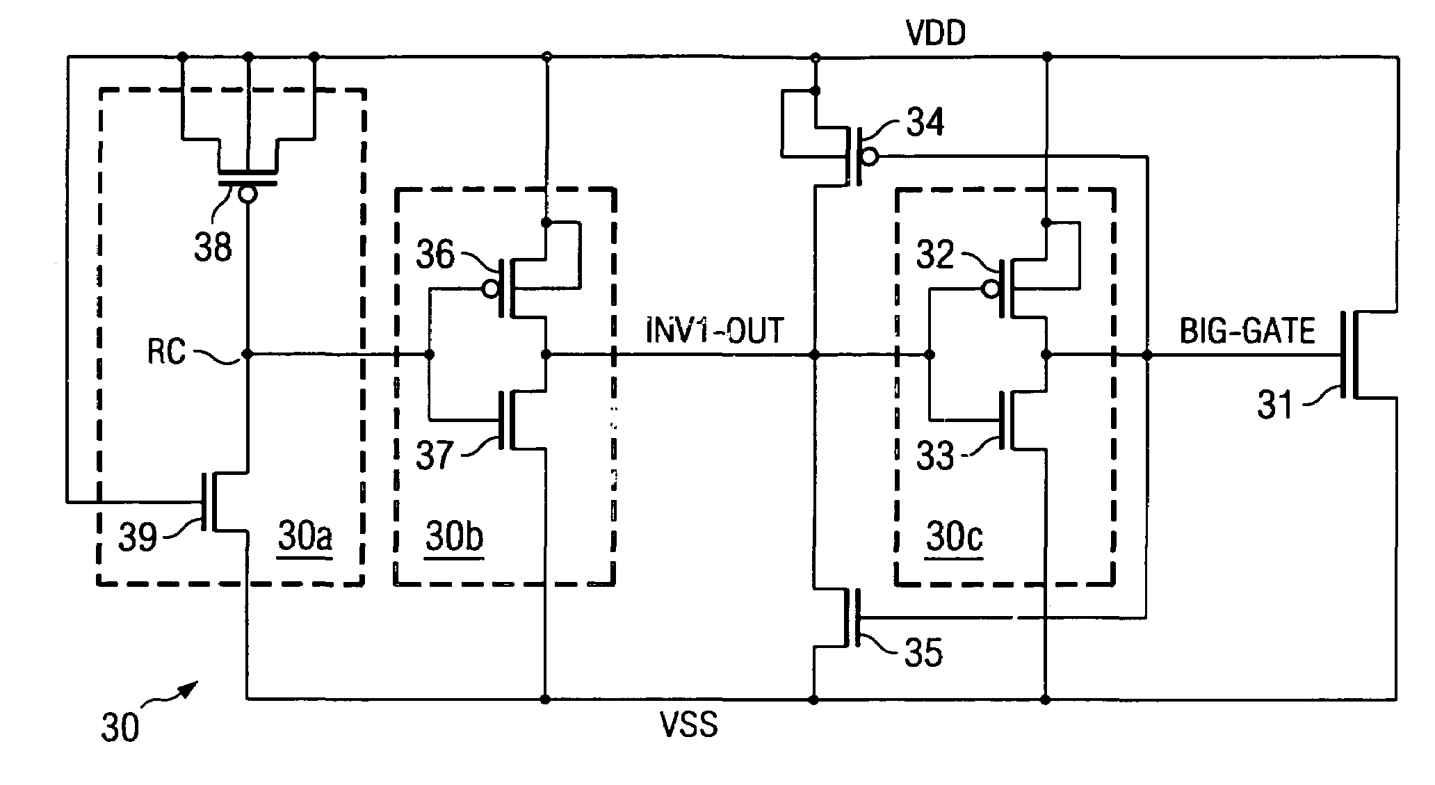
[0022]FIG. 4 depicts a schematic diagram of the rail clamp circuit of this invention. The circuit is comprised of an RC circuit 30a (timing circuit), a first inverter circuit 30b (CMOS inverter), a second inverter circuit 30c (CMOS inverter), an ESD transistor 31 (ESD device), a feedback NMOS device 35 and a feedback PMOS device 34. The RC circuit 30a, is further comprised of PMOS transistor 38 that functions as a capacitor and NMOS transistor 39 which functions as a resistor. PMOS transistor 38 has its first and second current electrodes, and its well electrode coupled to the VDD supply rail. The control electrode of transistor 38 is coupled to node RC. The NMOS transistor 39 has its source electrode coupled to the VSS rail and its drain electrode coupled to node RC. The control electrode of transistor 39 is coupled to the node VDD. Inverter 30b is comprised of PMOS transistor 36 and NMOS transistor 37. PMOS transistor 36 has its source and well terminal coupled to the rail VDD, it...


PUM


Abstract

A feedback enhanced triggering device for an electrostatic discharge protection circuit includes: a first inverter 30b having an output coupled to an input of a second inverter 30c, the second inverter 30c having an output coupled to a control node for a discharge device 31 such as a transistor; a high side feedback transistor 34 coupled to the output of the first inverter 30b, and having a control node coupled to the output of the second inverter 30c; and a low side feedback transistor 35 coupled to the output of the first inverter 30b, and having a control node coupled to the output of the second inverter 30c, wherein the feedback transistors 34 and 35 provide enhanced triggering for electrostatic discharge protection.

Description

FIELD OF THE INVENTION[0001]This invention generally relates to electronic systems and in particular it relates to electrostatic discharge protection circuits.BACKGROUND OF THE INVENTION[0002]FIG. 1 depicts a circuit diagram of a portion of an electrostatic discharge (ESD) protection circuit 10 that contains an Input / Output (I / O) pad 20. The I / O pad 20 further contains bondpad 24, diodes 25 and 26, and MOSFETS 27 and 28. Within this specification the first current electrode of MOSFET devices is called the source terminal, which is coupled to one of the power supply terminals VDD or VSS unless otherwise specified. The second current electrode of those same MOSFET devices is called the drain terminal. The drain terminal of MOSFET 28 is coupled to bondpad 24, as is the drain terminal of MOSFET 27. In I / O pad 20, the anode of diode 26 is coupled to bondpad 24 and the cathode of diode 26 is coupled to supply terminal VDD. Similarly, the cathode of diode 25 is coupled to the bondpad 24 an...

Claims


Application Information

Patent Timeline
Patent Type & Authority Patents(United States)
IPC IPC(8): H02H9/00H01L27/02
CPCH01L27/0251
Inventor SMITH, JEREMY C.
Owner TEXAS INSTR INC
Why Eureka
Try Eureka