Method for fabricating semiconductor device

a semiconductor and device technology, applied in the direction of semiconductor devices, capacitors, electrical equipment, etc., can solve the problems of zigzag arrangement of lower electrodes, electric short between lower electrodes, and additional cost, so as to prevent electric short, increase the effective capacitor area, and ensure the capacitance of capacitors

Active Publication Date: 2006-04-18
SK HYNIX INC
View PDF9 Cites 13 Cited by
  • Summary
  • Abstract
  • Description
  • Claims
  • Application Information

AI Technical Summary

Benefits of technology

[0072]It is, therefore, an object of the present invention to provide a method for fabricating a semiconductor device capable of preventing an electric short between lower electrodes caused by leaning lower electrodes, or lifted lower electrodes and of securing a sufficient capacitance of a capacitor by increasing an effective capacitor area.

Problems solved by technology

In this case, however, there may be a problem of an electric short between the lower electrodes 22 because of leaning lower electrodes 22 resulted from an interfacial tension created by the use of BOE or HF in the wet dip-out process.
Thus, an additional cost is necessary.
Nevertheless, this attempt to arrange the lower electrodes in the form of a zigzag has disadvantages.
First, as a pattern becomes micronized, it is difficult to prevent the pattern from collapsing.
Also, another factor that may cause the pattern to collapse is that the lower electrodes become lifted, further resulting in an electric short between the lower electrodes.
Thus, in the major axis, an inclined etch profile is obtained, resulting in a decrease in an effective surface area of a capacitor.
As a result, when metastable polysilicon (MPS) grains are grown for the purpose of increasing a capacitance of the capacitor, it is difficult to completely form MPS grains, a dielectric layer and an upper electrode because of an electric short between the MPS grains at a bottom part of the lower electrode.
If an over-etching process is adopted to obtain a vertical etch profile of the major axis, a sacrificial insulation layer in the minor axis is excessively etched, resulting in a bowing profile, which causes the electric short between the lower electrodes as shown in FIG. 3.
As a result of this decreased contact area, there is a high chance that the lower electrode will lift during the wet dip-out process or other subsequent process.
Because of the decreased critical dimension, a thickness of the lower electrode is also decreased, further increasing a chance of a broken lower electrode.
Eventually, this decrease in the effective capacitor area may result in a difficulty in securing the capacitance.
However, the pattern collapse phenomenon expressed with a reference denotation Y still occurs due to a limitation in process resulted from large scale integration and a bowing profile caused by a difference between etch profiles of a major axis and a minor axis. FIG. 7C shows that the pattern collapse phenomenon is not observed when circular lower electrodes 70C are arranged in the form of zigzag.
However, this suggested condition may not fundamentally prevent the bridge formation between the lower electrodes caused by the leaning phenomenon.

Method used


Image

  • Method for fabricating semiconductor device
  • Method for fabricating semiconductor device
  • Method for fabricating semiconductor device

Examples


Embodiment Construction

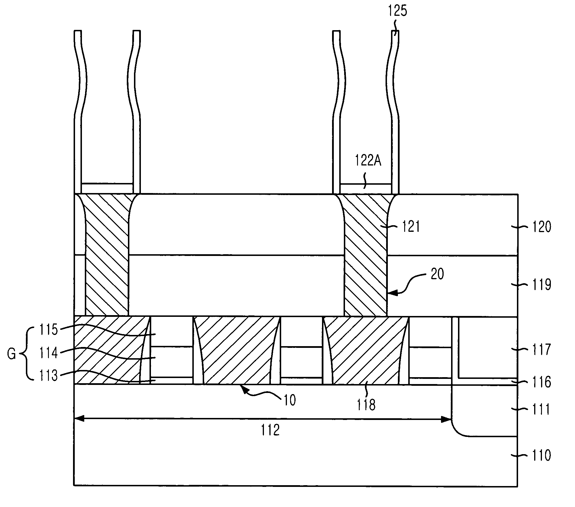
[0095]A method for fabricating a semiconductor device in accordance with a preferred embodiment of the present invention will be described in detail with reference to the accompanying drawings.

[0096]FIG. 11 is a top view showing a semiconductor memory device having a structure of one transistor-one capacitor (1T1C) in accordance with a preferred embodiment of the present invention.

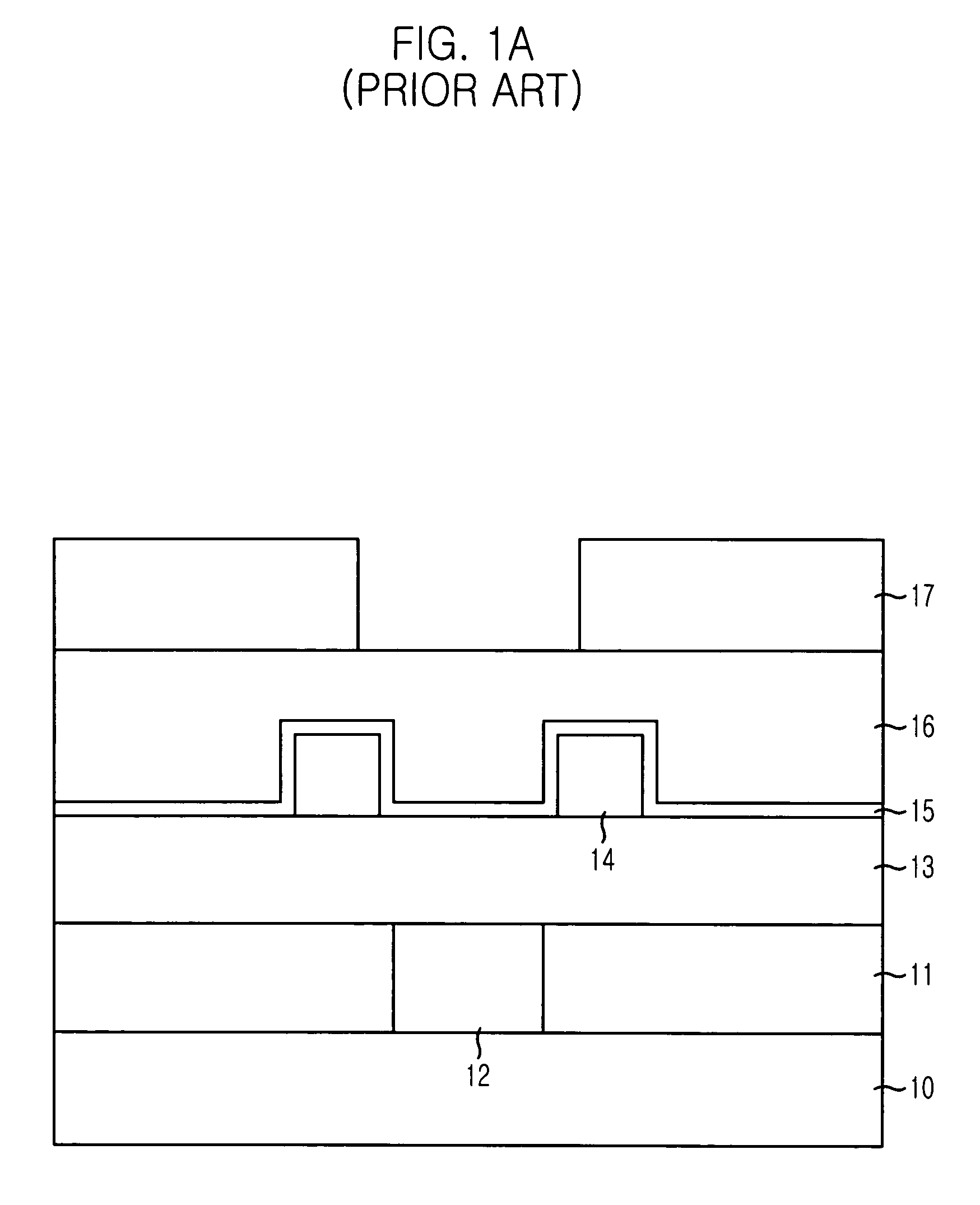
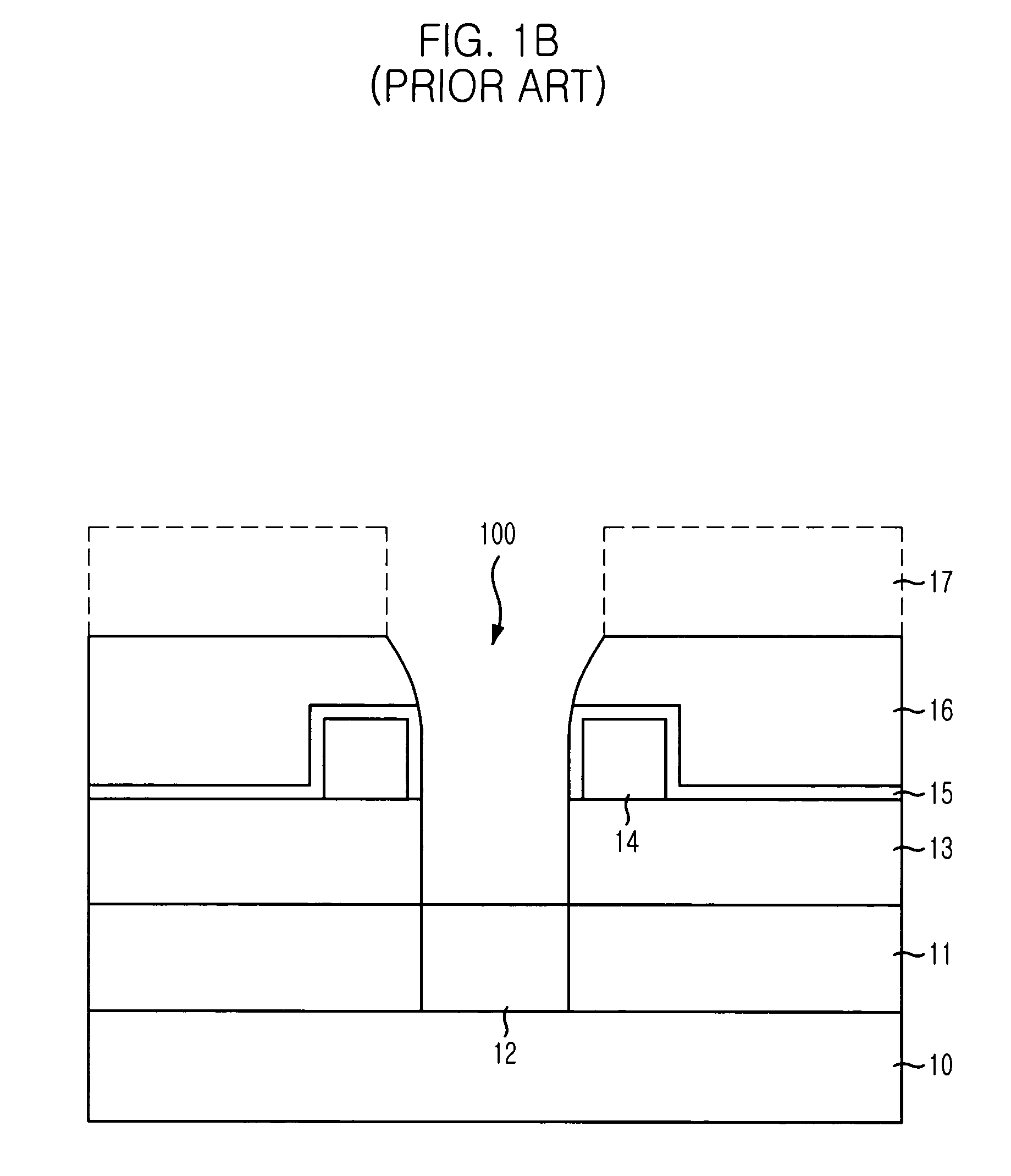
[0097]As shown, a plurality of gate electrodes, for instance, first to third word lines WL1, WL2 and WL3, are arranged in one direction. A first bit line BL1 and a second bit line BL2 are arranged in a crossing direction to the first to the third word lines WL1 to WL3. Also, there is a landing plug contact LPC1. Herein, the landing plug contact LPC1 is made of polysilicon. Also, although not illustrated, the landing plug contact LPC1 is connected to a substrate through a contact hole formed by using a T-type mask pattern exposing a predetermined portion of the substrate, e.g., an impurity diffusion region....


PUM


Abstract

A method for fabricating a semiconductor device capable of preventing an electric short between lower electrodes caused by leaning lower electrodes, or lifted lower electrodes and of securing a sufficient capacitance of a capacitor by increasing an effective capacitor area. The method includes the steps of: preparing a semi-finished semiconductor substrate; forming a sacrificial layer on the semi-finished semiconductor substrate; patterning the sacrificial layer by using an island-type photoresist pattern, thereby obtaining at least one contact hole to expose portions of the semi-finished semiconductor substrate; and forming a conductive layer on the sacrificial layer.

Description

FIELD OF THE INVENTION[0001]The present invention relates to a method for fabricating a semiconductor device; and, more particularly, to a method for fabricating a lower electrode of a capacitor in a semiconductor device.DESCRIPTION OF RELATED ARTS[0002]A recent progression in micronization in semiconductor technology has led to acceleration in achieving a large-scale of integration of a memory device. As a result, a unit cell area is decreased and a required operation voltage becomes low. Although the unit cell area is decreased, it is required to have a capacitance greater than 25 fF per cell in order to prevent incidences of soft error and shortened refresh time. Therefore, there have been diverse approaches to secure a required capacitance.[0003]One approach for securing a required capacitance is to form a capacitor in three dimensions. Typical examples of three-dimensional capacitor are a concave-type capacitor and a cylinder-type capacitor.[0004]FIGS. 1A to 1D are cross-sectio...

Claims


Application Information

Patent Timeline
Patent Type & Authority Patents(United States)
IPC IPC(8): H01L21/8242H01L21/28H01L21/02H01L21/768H01L21/8239H01L27/02H01L27/108
CPCH01L27/1052H01L28/91H01L27/10852H01L27/0207H01L27/10814H10B99/00H10B12/315H10B12/033
Inventor AHN, MYUNG-KYU
Owner SK HYNIX INC
Why Eureka
Try Eureka