Integrated circuit die and/or package having a variable pitch contact array for maximization of number of signal lines per routing layer

a technology of contact array and integrated circuit, which is applied in the direction of printed circuit, sustainable manufacturing/processing, final product manufacturing, etc., can solve the problems of limiting the number of signal traces that can be fabricated, limiting the spacing between the vias, and complicated packaging of integrated circuits

Inactive Publication Date: 2006-04-18
INTEL CORP
View PDF14 Cites 3 Cited by
  • Summary
  • Abstract
  • Description
  • Claims
  • Application Information

AI Technical Summary

Benefits of technology

[0010]The present invention discloses an integrated circuit die and / or package. In both cases, the package and / or die have a substrate with a central region and an outer region. A first plurality of electrical connections is spaced apart by a first distance on the outer region of the substrate. A second plurality of electrical connections is spaced apart by a second distance, smaller than the first distance, on the central region of the substrate.

Problems solved by technology

As integrated circuits become more dense and therefore smaller, the packaging of integrated circuit becomes more complex.
However, various constraints limit the number of signal traces that can be fabricated on an integrated circuit die or package using an array layout.
Industry standards and other process issues impose specific requirements as to the spacing between electrical contacts (e.g., electrically conductive bumps such as solder bumps), thereby restricting the spacing between the vias that electrically connect the signal traces to the solder bumps.
The limitation on the maximum number of usable signal traces limits the maximum number of solder bumps, thereby placing a ceiling on the number of signals that a particular die and / or package can provide.

Method used


Image

  • Integrated circuit die and/or package having a variable pitch contact array for maximization of number of signal lines per routing layer
  • Integrated circuit die and/or package having a variable pitch contact array for maximization of number of signal lines per routing layer
  • Integrated circuit die and/or package having a variable pitch contact array for maximization of number of signal lines per routing layer

Examples


Embodiment Construction

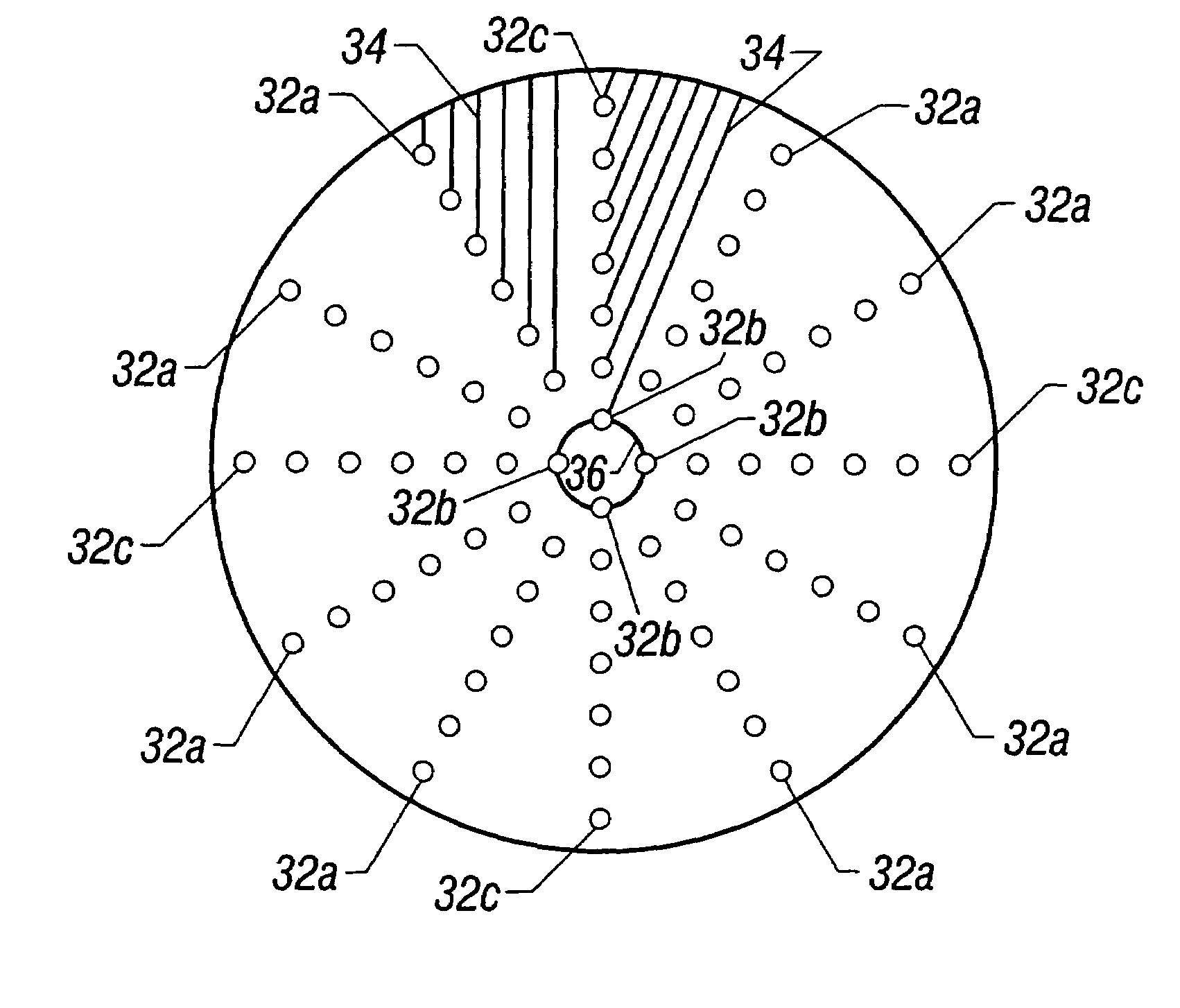
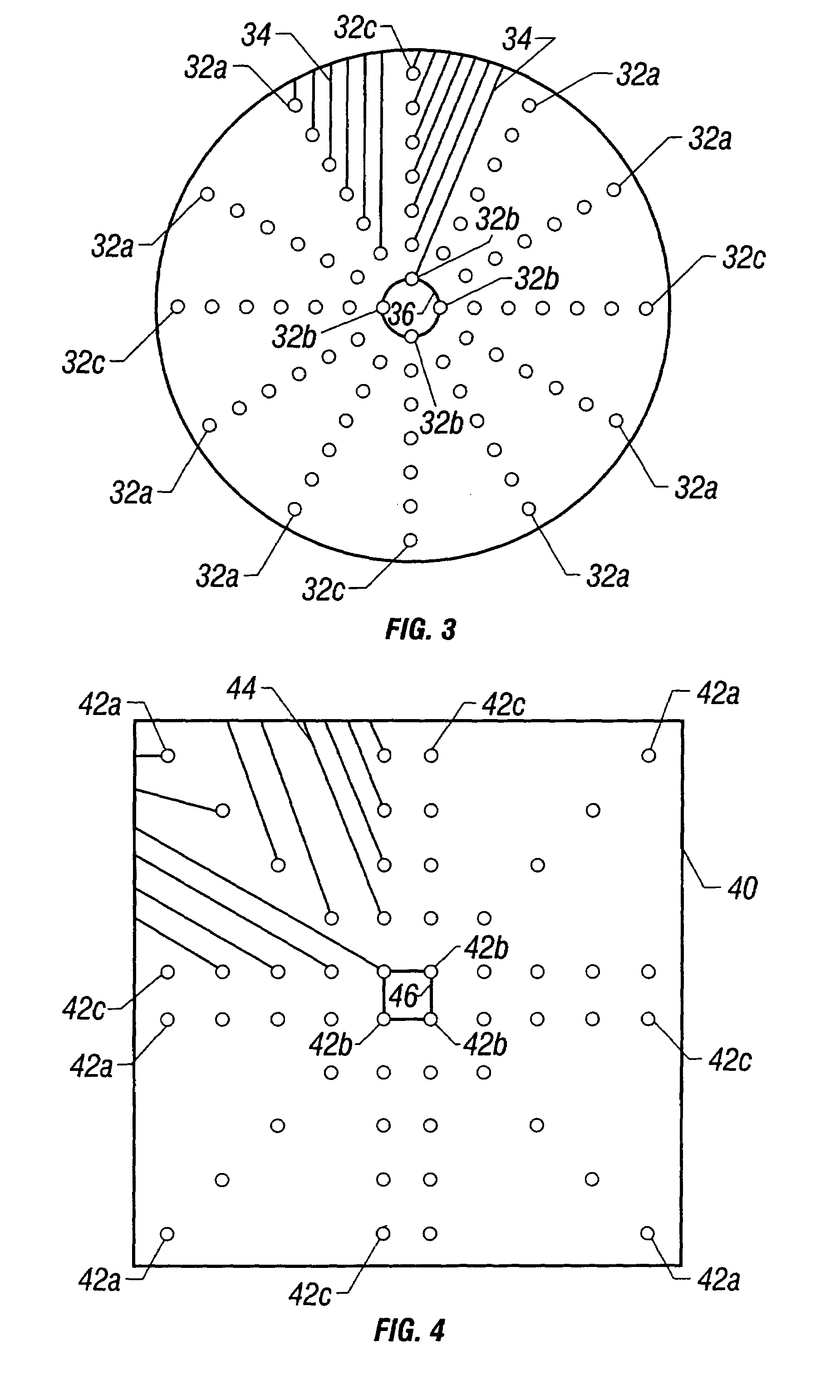
[0016]The present invention discloses to a grid array layout having a progressively variable pitch to enable a maximum number of signal lines to be routed through the grid layout. In the following description, numerous specific details are set forth such as specific materials, process parameters, dimensions, etc. in order to provide a thorough understanding of the present invention. It will be obvious, however, to one skilled in the art that these specific details need not be employed to practice the present invention. In other instances, well-known materials or methods have not been described in detail in order to avoid unnecessarily obscuring the present invention.

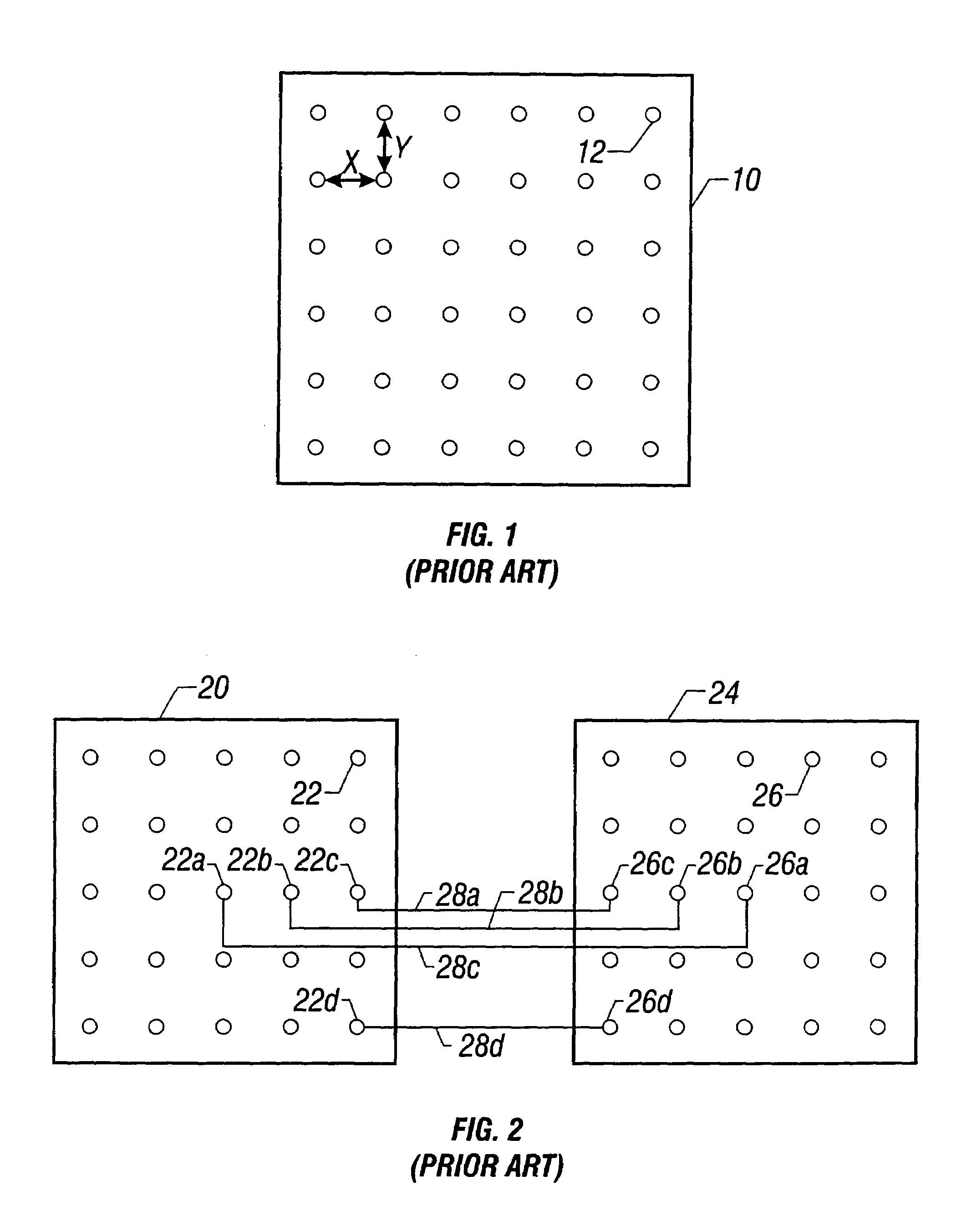
[0017]An electrical apparatus generally has a substrate with numerous points of electrical contact with signal traces extending from each point of electrical contact to provide paths for electrical connections between, for example, an IC die and a package between IC packages, between an IC package and a printed circuit b...


PUM


Abstract

An integrated circuit die and/or package. An apparatus is described having a substrate with a central region and an outer region. A first plurality of electrical connections is spaced apart by a first distance on the outer region of the substrate. A second plurality of electrical connections is spaced apart by a second distance, smaller than the first distance, on the central region of the substrate.

Description

[0001]This is a Divisional Application of Ser. No.: 09 / 342,550 filed Jun. 29, 1999, now U.S. Pat. No. 6,664,620.BACKGROUND OF THE INVENTION[0002]1. Field of the Invention[0003]The present invention relates to the field of integrated circuits and packages. More particularly, the present invention relates to an integrated circuit and / or a grid array package having a progressively variable pitch.[0004]2. Description of Related Art[0005]Over the years, the electronics industry has minimized the size of integrated circuit chip designs. As integrated circuits become more dense and therefore smaller, the packaging of integrated circuit becomes more complex. As a consequence, more and more input and output (I / O) connections become available for use with a single integrated circuit. For example, an integrated circuit with a size of 0.5 inches square can easily require 400 or more connections.[0006]Some of the latest microprocessor devices are packaged in land grid array (LGA) packages or mod...

Claims


Application Information

Patent Timeline
Patent Type & Authority Patents(United States)
IPC IPC(8): H01L23/42H01L23/52H01L29/40H01L23/12H05K3/34H01L23/498H05K1/11
CPCH01L23/49811H01L23/49838H05K1/111H05K2201/09418H01L2924/0002H05K2201/10734H01L2924/00Y02P70/50
Inventor SIU, WILLIAM M.BHATTACHARYYA, BIDYUT K.
Owner INTEL CORP
Why Eureka
Try Eureka