Water soluble negative tone photoresist

a negative tone and photoresist technology, applied in the field of manufacturing integrated circuits, can solve the problems of cumbersome generation of opcs and the dependence of space width wb>1/b>, and achieve the effect of shrinking the size of unplugged holes

Inactive Publication Date: 2006-04-25
TAIWAN SEMICON MFG CO LTD
View PDF12 Cites 16 Cited by
  • Summary
  • Abstract
  • Description
  • Claims
  • Application Information

AI Technical Summary

Benefits of technology

[0017]A further objective of the present invention is to provide a method of shrinking the space width of a hole or trench that has been patterned by UV radiation including sub-200 nm wavelengths or by e-beam exposure where the space width has a size that can be as small as 130 nm or less.
[0019]Yet another objective of the present invention is to provide a negative tone resist that may be coated over an existing photoresist pattern to simultaneously adjust the print density in the pattern and shrink the space width of holes or trenches in the pattern.
[0022]The second patterned layer comprised of the thin crosslinked layer and the crosslinked plugs has holes with a second space width that is less than the first space width in the first patterned layer. The thin crosslinked layer effectively shrinks the size of unplugged holes in the first patterned resist layer by forming a liner on the sidewalls of the unplugged holes. The thickness of the thin crosslinked layer and therefore the second space width may be controlled by the amount of quencher in the negative resist and the PEB conditions. The second patterned layer serves as an etch mask while the hole pattern in the second patterned layer is transferred into the substrate. The pattern density is adjusted since the crosslinked plugs prevent unwanted holes from being transferred into the substrate during the etch step. The first patterned resist layer and the second patterned resist layer are stripped and the substrate is ready for subsequent processing.
[0026]The second patterned resist layer effectively shrinks the size of unplugged holes in the first patterned resist layer by forming a liner on the sidewalls of the unplugged holes. The thickness of the second patterned resist layer and therefore the second space width can be controlled by the amount of quencher in the water soluble negative resist and the PEB conditions. The second patterned resist layer serves as an etch mask while the hole pattern in the second patterned resist layer is transferred into the substrate. The pattern density is adjusted since the water insoluble plugs prevent unwanted holes from being transferred into the substrate during the etch step. The first patterned resist layer and the second patterned resist layer are stripped and the substrate is ready for subsequent processing.

Problems solved by technology

One of the problems associated with a typical patterning process is that space width W1 is dependent on pattern density.
OPC can be cumbersome to generate and a period of one or two months may be necessary before a new mask with OPC corrections is available.
However, the crosslinking layer does not contain a quencher and the extent of acid diffusion is determined by only the bake temperature and time which may be difficult to reproduce uniformly across a wafer.

Method used


Image

  • Water soluble negative tone photoresist
  • Water soluble negative tone photoresist
  • Water soluble negative tone photoresist

Examples


first embodiment

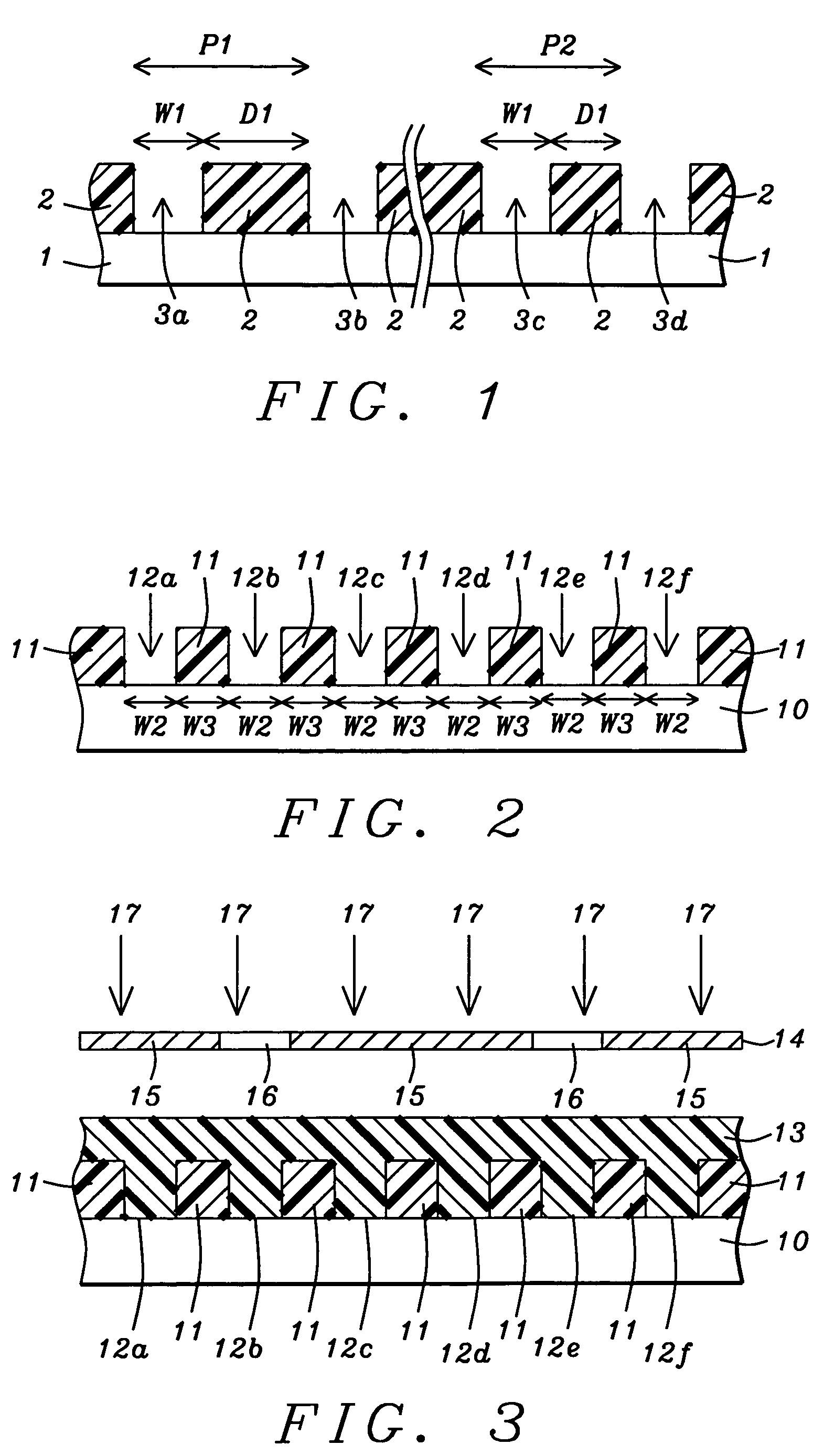
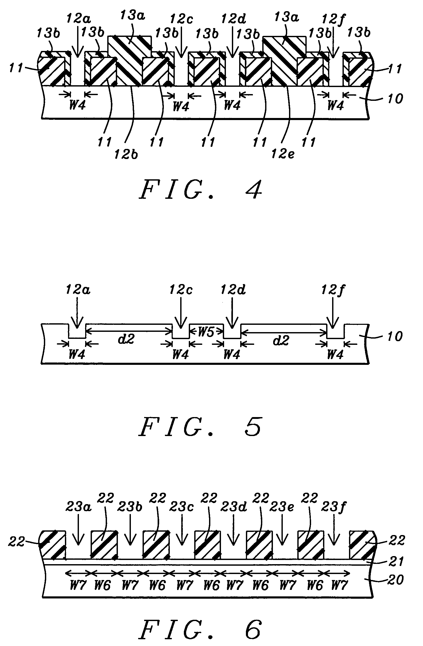
[0030]The present invention is described with reference to the drawings which are not necessarily drawn to scale and are provided by way of example and not intended to limit the scope of the invention. In the first embodiment as illustrated in FIGS. 2–5, a method is described for shrinking the space width of holes in a resist pattern while simultaneously reducing the pattern density of the holes in the pattern. This method allows holes with the same space width but different pattern densities to be formed in a pattern in a resist layer that is transferred into a substrate. The holes may be vias, contact holes, trenches, or other features which have a space width to be decreased and a pattern density to be reduced.

[0031]Referring to FIG. 2, a substrate 10 is provided that may contain active and passive devices in a substructure that is not shown in order to simply the drawing and direct attention to the present invention. In one embodiment, an anti-reflective coating or ARC (not show...

second embodiment

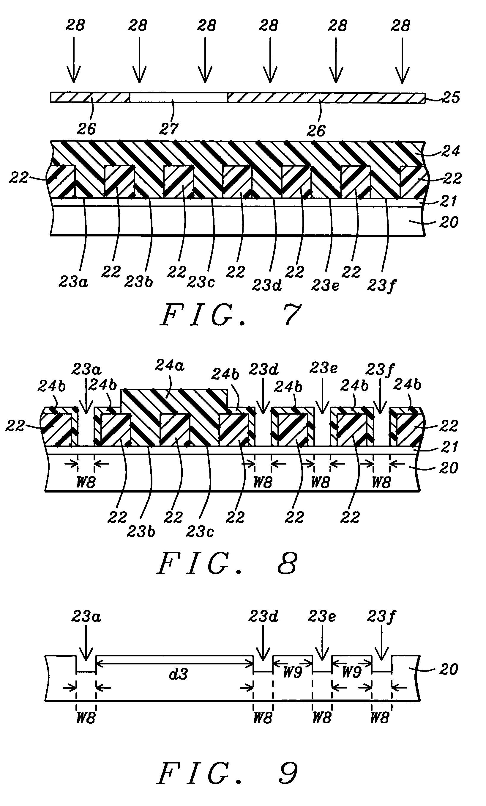
[0056]In a second embodiment illustrated in FIGS. 6–9, a method is described that relates to shrinking the space width of holes in at least two regions of a first resist pattern having equal pattern densities and equal space widths whereby a second pattern is formed in a substrate in which the two regions have holes with different pattern densities but equal and smaller space widths. In other words, a reduced pattern density is formed in at least one of the substrate regions and all holes formed in the substrate have reduced space widths compared to the first resist pattern.

[0057]Referring to FIG. 6, a substrate 20 is provided that is typically comprised of silicon and may contain active and passive devices in a substructure that is not shown in order to simply the drawing. An anti-reflective coating (ARC) 21 is formed on the substrate 20 in order to control reflectivity during a subsequent resist patterning process. The ARC 21 may be an inorganic material such as silicon nitride or...


PUM

PropertyMeasurementUnit
wavelengthsaaaaaaaaaa
feature sizeaaaaaaaaaa
wavelengthsaaaaaaaaaa

Abstract

A method is described for reducing the space width of holes in a first resist pattern and simultaneously removing unwanted holes to change the pattern density in the resulting second pattern. This technique provides holes with a uniform space width as small as 100 nm or less that is independent of pattern density in the second pattern. A positive resist is patterned to form holes with a first pattern density and first space width. A water soluble negative resist is coated over the first resist and selectively exposed to form a second patterned layer consisting of water insoluble plugs in unwanted holes in the first pattern and a thin water insoluble layer on the first resist pattern in unexposed portions. The plugs may form dense and isolated hole arrays while the thin insoluble layer reduces space width to the same extent in remaining holes in the second pattern.

Description

RELATED PATENT APPLICATIONS[0001]This application is related to the following: Ser. No. 10 / 002,986, filing date Nov. 30, 2001; Ser. No. 10 / 005,806, filing date Dec. 5, 2001; Ser. No. 10 / 443,359, filing date May 22, 2003; and Ser. No. 10 / 268,586, filing date Oct. 10, 2002, all assigned to a common assignee.FIELD OF THE INVENTION[0002]The invention relates to a method of fabricating an integrated circuit in a semiconductor device. More particularly, the present invention relates to a method of reducing hole or trench sizes in a photoresist pattern and for optimizing the print density of said pattern.BACKGROUND OF THE INVENTION[0003]Photoresist patterning is a key step in the formation of integrated circuits in semiconductor devices. A photoresist, hereafter referred to as resist, is typically spin coated on a substrate, baked to form a film, and patternwise exposed by employing an exposure tool and a mask that contains a device pattern. Radiation is transmitted through transparent reg...

Claims


Application Information

Patent Timeline
Patent Type & Authority Patents(United States)
IPC IPC(8): G03C1/735G03C5/00G03F7/00G03F7/038G03F7/40
CPCG03F7/0035G03F7/40G03F7/038
Inventor HO, BANG-CHIENCHEN, JIAN-HONG
Owner TAIWAN SEMICON MFG CO LTD
Why Eureka
Try Eureka