Apparatus and method for thermal isolation, circuit cooling and electromagnetic shielding of a wafer

a technology of electromagnetic shielding and circuit cooling, applied in electrical apparatus, semiconductor devices, semiconductor/solid-state device details, etc., can solve the problems of inability to close the integration of laser drivers and laser diodes on the same silicon substrate, complicated system integration and packaging, and limited substrate choice for laser diodes to be mounted, etc., to achieve the effect of preventing noise (thermal or electromagnetic) transmission

Active Publication Date: 2006-04-25
TWITTER INC
View PDF2 Cites 75 Cited by
  • Summary
  • Abstract
  • Description
  • Claims
  • Application Information

AI Technical Summary

Benefits of technology

[0004]In one embodiment, the disclosure is directed to a system-on-chip where a first region is thermally isolated from a second region by a thermal barrier in the form of a maze of through wafer vias. The barrier region defines a thermal path between the first region and the second region. To extend the thermal path, the region may have a plurality of vias formed thereon in the shape of a maze. The maze of through-vias lengthen the thermal path between the two regions so thermal resistance between the regions is increased. In an exemplary embodiment, the two regions may comprise two circuits built on the same substrate. In another exemplary embodiment, two region are formed on a carrier onto which the chips are flipped bonded.
[0006]In still another embodiment, the disclosure relates to a method for thermo-electrically shielding a sensitive region of a semiconductor wafer by defining a first and a second region on the semiconductor, the first region generating thermo-electrical noise which conducts through a thermal path to the second region. A barrier region may be formed the substrate to separate the two regions. The barrier region may have a plurality of discrete vias extending through a cross section of the substrate to thereby lengthen the thermal path between the regions. The vias may be configured to have a pattern in order to extend the thermal path between the regions. The barrier between the regions may be formed by etching a trench by removing the wafer material in the trench region such that the trench bottom reaches a handle substrate. Optionally, the trench may be filled with a non-conductive material and the handle substrate may be then removed.
[0009]In another embodiment, an SOI wafer is attached to a thermally non-conductive substrate. The SOI wafer may be thinned by removing or grinding a portion thereof. The remaining silicon can be selectively etched using BOX as an etch-stop layer. A thermal barrier between two regions of the remaining SOI film may then be formed by etching a trench that separates the two regions. The trench may optionally reach the thermally non-conductive substrate. Finally, the trench may be filled with a non-conductive material and planarized to further deter noise (thermal or electromagnetic) transmission between the two regions.

Problems solved by technology

Physical separation, however, complicates system integration and packaging.
Moreover, to reduce losses the transmission lines should be made on insulating substrates which further limit the choice of substrate on which the laser diode may be mounted.
Because silicon is a good heat conductor, the close integration of the laser driver and the laser diode on the same silicon substrate is not possible for the reasons explained above.
Digital components tend to be noisy and disturb the performance of sensitive low-noise RF or analog components.

Method used


Image

  • Apparatus and method for thermal isolation, circuit cooling and electromagnetic shielding of a wafer
  • Apparatus and method for thermal isolation, circuit cooling and electromagnetic shielding of a wafer
  • Apparatus and method for thermal isolation, circuit cooling and electromagnetic shielding of a wafer

Examples


Embodiment Construction

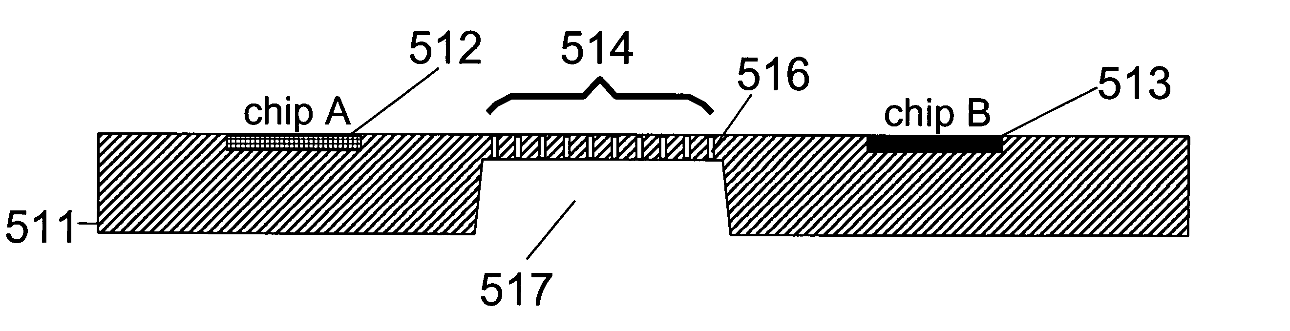
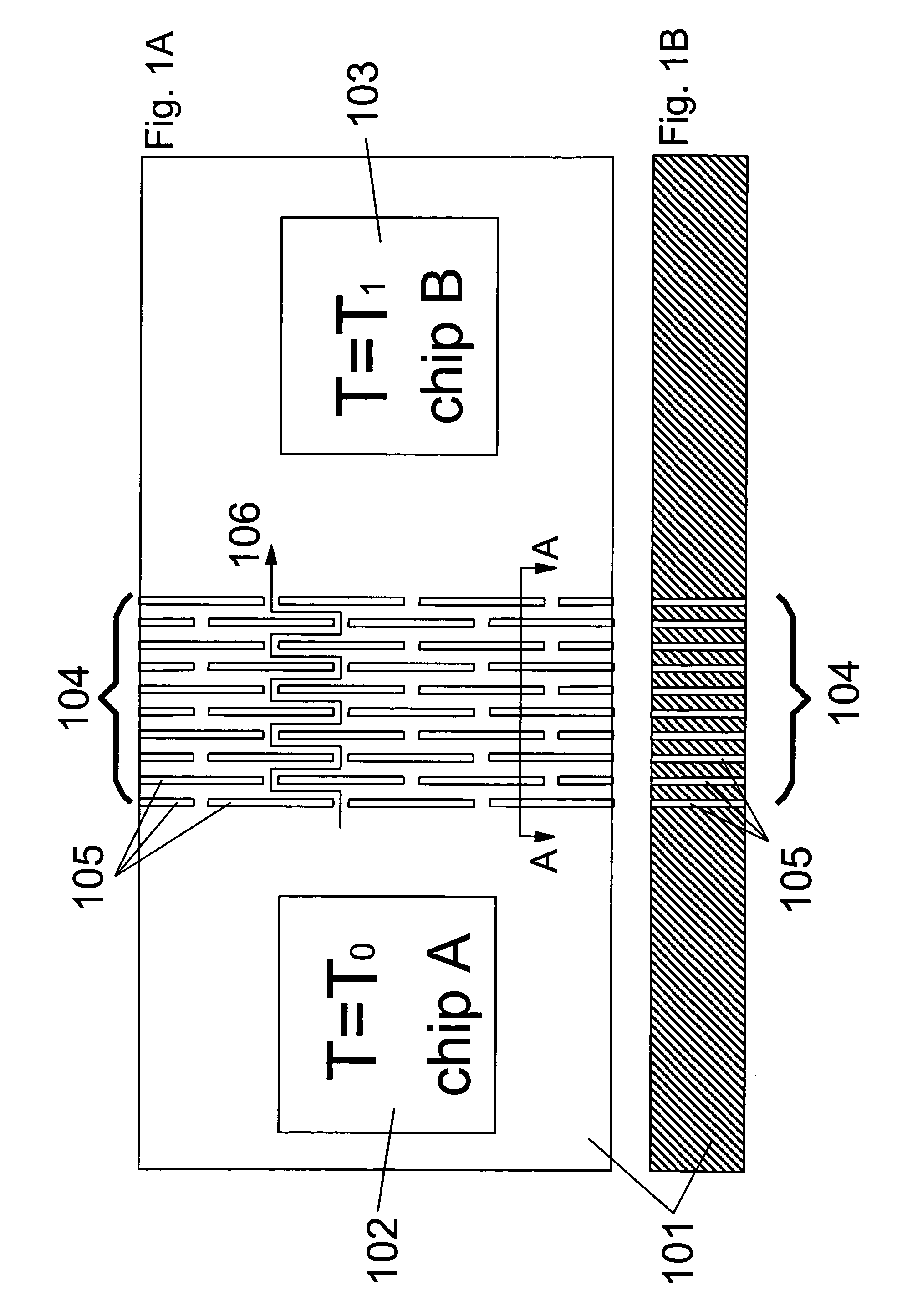
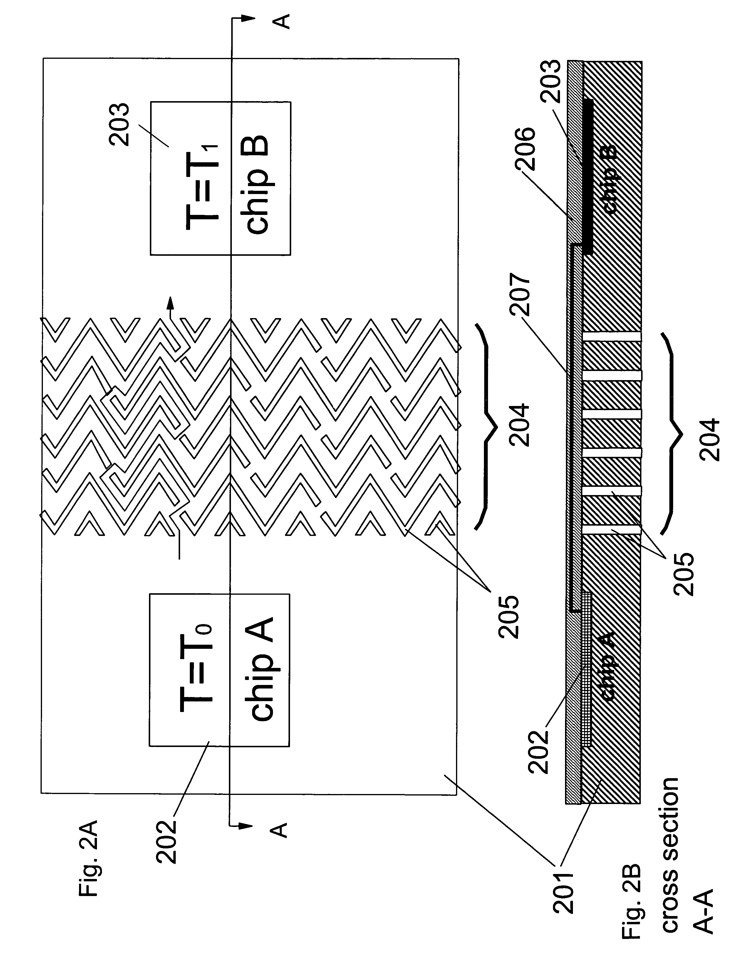
[0022]FIGS. 1A and 1B show a silicon substrate 101 including chip A occupying region 102, chip B occupying region 103 and a thermal barrier 104 separating the two regions. The term “chip” as used herein, generally refers to a semiconductor wafer mounted on the substrate 101 or alternatively to a circuit fabricated in the silicon substrate 101. The thermal barrier includes through vias 105 devised to form a maze-type structure. The maze of through-vias 105 lengthen the thermal path between chip A 102 and chip B 103 as illustrated by arrow 106. In the exemplary embodiment of FIG. 1, thermal impedance is increased since vias 105 are poor thermal conductors and since conduction primarily occurs in the solid portion of maze 104 as indicated by the arrow 106. FIG. 1B shows a cross sectional view of substrate 101 having through vias 105 formed thereon. Thus, in accordance with one embodiment of the disclosure, thermal isolation may be enhanced by lengthening the conductive thermal path.

[00...


PUM


Abstract

The disclosure relates to method and apparatus for isolating sensitive regions of a semiconductor device by providing a thermal path or an electromagnetic shield. The thermal path may include vias having different length, depth and configuration such that the thermal path between the two regions is lengthened. In addition, the vias may be fully or partially filled with an insulating material having defined conductive properties to further retard heat electromagnetic or heat transmission between the regions. In another embodiment, electrical isolation between two regions is achieved by etching a closed loop or an open loop trench at the border of the regions and filling the trench with a conductive material to provide proper termination of electromagnetic fields within the substrate.

Description

BACKGROUND[0001]The operation of semiconductor devices such as laser diodes and photodiodes is sensitive to the device temperature. For example, the laser emission wavelength will typically shift as the device temperature rises. This shift is undesirable and, for optimal results, should be avoided. In many applications the laser diode is mounted on a separate substrate than that of the electronics that drives the laser. Physical separation is required so that the power dissipated by the laser driver circuit does not heat the laser diode. Physical separation, however, complicates system integration and packaging. For example, since separate substrates are used for mounting the laser and the laser driver chip, long wire traces are required to electrically connect the two together. The design of such wire (typically referred to as transmission lines at the frequency of operation) is not trivial. Moreover, to reduce losses the transmission lines should be made on insulating substrates w...

Claims


Application Information

Patent Timeline
Patent Type & Authority Patents(United States)
IPC IPC(8): H01L21/4763H01L21/76H01L23/367
CPCH01L23/3677H01L23/552H01L2924/3011H01L2924/0002H01L2924/00
Inventor COHEN, GUY M.EDELSTEIN, DANIEL C.JENKINS, KEITH A.PATEL, CHIRAG S.SHAN, LIE
Owner TWITTER INC
Why Eureka
Try Eureka