Thin planar semiconductor device having electrodes on both surfaces and method of fabricating same

Inactive Publication Date: 2006-04-25
RENESAS ELECTRONICS CORP
View PDF8 Cites 68 Cited by
  • Summary
  • Abstract
  • Description
  • Claims
  • Application Information

AI Technical Summary

Benefits of technology

[0007]It is an object of the present invention to provide a novel semiconductor device and a method of fabricating the semiconductor device that can provide a

Problems solved by technology

In actuality, however, the simultaneous formation of various function blocks requiring different forming processes on a silicon wafer is problematic both in terms of design as well as fabri

Method used


Image

  • Thin planar semiconductor device having electrodes on both surfaces and method of fabricating same
  • Thin planar semiconductor device having electrodes on both surfaces and method of fabricating same
  • Thin planar semiconductor device having electrodes on both surfaces and method of fabricating same

Examples


second embodiment

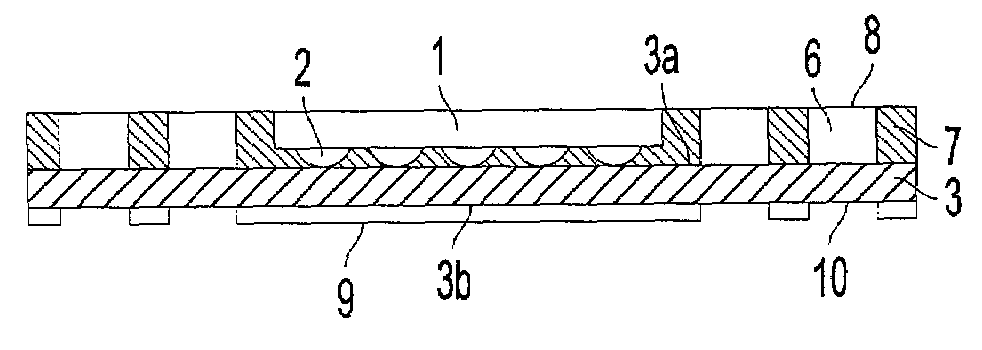
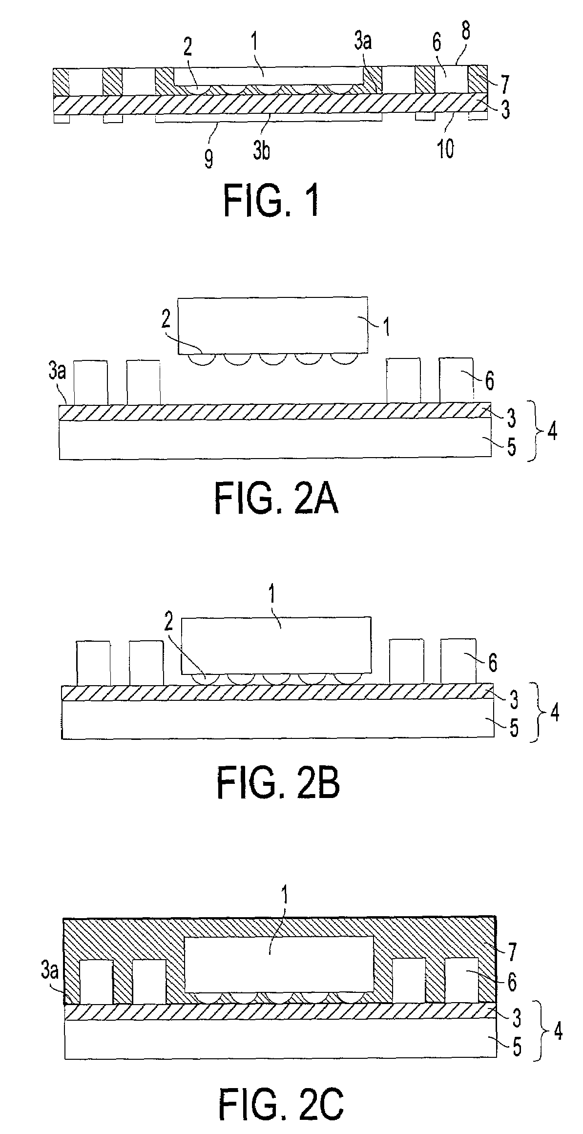
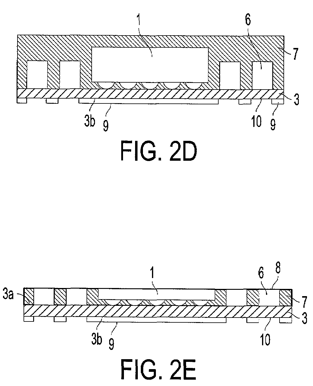
[0043]The semiconductor device of the second embodiment that is shown in FIG. 3 is an assembled unit in which three of the semiconductor devices shown in FIG. 1 are stacked and electrically interconnected. Although there are three stacked layers in FIG. 3, the present invention is not limited to this number.

[0044]Referring now to FIG. 3, among vertically stacked semiconductor devices 13, exposed portions 10 of wiring layer 3 that are not covered by solder resist layer 9 of one semiconductor device 13 are connected by solder 11 to end surfaces 8 of conductive posts 6 that are provided on wiring layer 3 of another semiconductor device 13. In addition, ball-shaped solder 12 is affixed as electrode terminals to exposed portions 10 of wiring layer 3 that are not covered by solder resist layer 9 of lowermost semiconductor device 13.

[0045]Ball-shaped solder may also be affixed as electrode terminals to end surfaces 8 of conductive posts 6 of uppermost semiconductor device 13.

[0046]Stacking...

third embodiment

[0047]Explanation next regards the semiconductor device of the present invention.

[0048]The semiconductor device of the third embodiment that is shown in FIG. 4 is a structure in which planar wiring layer 14 made up by electrical wiring is provided on surface 15 that is on the opposite side from solder resist layer 9 of the semiconductor device shown in FIG. 1, this planar wiring layer 14 being electrically connected to end surfaces 8 of conductive posts 6.

[0049]In this construction, ball-shaped solder may be affixed as first electrode terminals to exposed portions 10 of the wiring of wiring layer 3 as shown in FIG. 3, and moreover, ball-shaped solder may be affixed as second electrode terminals to desired wiring of wiring layer 14. Of course, a construction is also possible in which second electrode terminals are not affixed to wiring layer 14.


PUM


Abstract

A thin, planar semiconductor device having electrodes on both surfaces is disclosed. This semiconductor device is provided with an IC chip and a wiring layer having one side that is electrically connected to surface electrodes of the IC chip. On this surface of the wiring layer, conductive posts are provided on wiring of the wiring layer, and an insulating resin covers all portions not occupied by the IC chip and conductive posts. The end surfaces of the conductive posts are exposed from the insulating resin and are used as first planar electrodes. In addition, a resist layer is formed on the opposite surface of the wiring layer. Exposed portions are formed in the resist layer to expose desired wiring portions of the wiring layer. These exposed portions are used as second planar electrodes. Stacking semiconductor devices of this construction enables an improvement in the integration of semiconductor integrated circuits.

Description

BACKGROUND OF THE INVENTION[0001]1. Field of the Invention[0002]The present invention relates to a semiconductor device and to a method of fabricating the semiconductor device, and in particular, to the construction of a semiconductor device that can be three-dimensionally stacked and to a method of fabricating the semiconductor device.[0003]2. Description of the Related Art[0004]With the rapid development of Internet technology, prior-art constructions such as mainframes and terminals that are connected to mainframes have been replaced by systems made up by servers that are distributed throughout the world and the high-speed communication lines that connect them.[0005]This information communication network is now rapidly coming into popular use in households and by individuals through inexpensive and highly functional personal computers or mobile telephones that can be connected to the Internet, and as a result, the next-generation Internet protocol (IPv6) will allow connection of ...

Claims


Application Information

Patent Timeline
IPC IPC(8): H01L21/44H01L25/065
CPCH01L25/0657H01L25/105H01L21/568H01L2224/16H01L2225/06517H01L2225/0652H01L2225/06541H01L2225/06572H01L2225/06582H01L2225/06586H01L2924/15311H01L2924/15331H01L2224/16225H01L2924/18161H01L2225/1035H01L2225/1058H01L2224/81005
Inventor KURITA, YOICHIRO
Owner RENESAS ELECTRONICS CORP
Why Eureka
Try Eureka