Versatile system for output energy limiting circuitry

a technology of output energy limiting circuitry and reverse circuitry, which is applied in the direction of pulse generator, power consumption reduction, pulse technique, etc., can solve the problems of reducing the efficiency of driver circuitry, reducing the efficiency of device and system inefficiency, and generating numerous challenges to the semiconductor manufacturing process. , to achieve the effect of limiting output energy levels, reducing device and system inefficiencies, and efficient and reliable device performan

Active Publication Date: 2006-04-25
TEXAS INSTR INC
View PDF5 Cites 2 Cited by
  • Summary
  • Abstract
  • Description
  • Claims
  • Application Information

AI Technical Summary

Benefits of technology

[0013]The present invention provides a versatile system, comprising various apparatus and methods, for limiting output energy levels across high-voltage driver circuitry, without over or under correction. The system of the present invention thereby reduces device and system inefficiencies commonly associated with conventional systems' excessive or inadequate off cycling of device output structures. The system of the present invention comprehends, and is readily adaptable to address, a wide variety of specific parametric requirements imposed by specific end-equipment applications. The present invention thus provides efficient and reliable device performance in an easy, cost-effective manner.
[0014]Specifically, the present invention provides circuitry that protects driver output structures (e.g., transistors) from exposure to excessive output energy levels that might otherwise damage or destroy those output structures. The circuitry of the present invention dynamically monitors both current and voltage levels across output structures to determine whether those output structures should be shut off to avoid exposure to excessive energy levels. The present invention recognizes that the energy across any given structure is a function of current, voltage and time. As an output structure experiences an overcurrent condition, the duration of the condition, and the magnitude of voltage across the output structure during the condition, determine whether the output structure is shut off. If an overcurrent condition exists, and the voltage across the output structure is relatively high, the output structure is shut off in a much shorter time than if the voltage across the output structure is relatively low. In such a manner, the present invention provides a dynamic deglitch time, which optimizes protection of output structures to a specific energy level limit, not just a selected current or voltage level threshold. This provides robust protection while efficiently accommodating temporary signal variances that commonly occur.

Problems solved by technology

The increased packing density of the integrated circuit generates numerous challenges to the semiconductor manufacturing process.
Often, such new applications place a number of unique demands on circuitry components and substructures.
Unfortunately, however, there are a large number of variables in semiconductor device manufacturing that can affect any given performance parameter.
Commonly, performance specifications require that driver circuitry consume relatively low power while driving a significant load.
Depending upon the design and fabrication processes used, however, certain adapted circuitry components may be susceptible to performance degradation or break down if non-standard conditions (e.g., overload, short) cause output circuitry to exceed the standard operating range.
For example, sustained power overload on certain output circuitry can cause a significant rise in operating temperature, which can—over time—begin to break down transistor structures.
Even over a relatively short amount of time, an excessive output energy drop can degrade the performance of output transistor structures, or render them completely inoperable.
In addition, increased energy drop across a driver output can significantly increase overall system power consumption.
This can cause a number of system inefficiency or reliability issues, or cause significant process yield problems for the device manufacturer.
Using such schemes, even instantaneous variations in current that exceed the threshold cause output shutdown—even though such variations may still be marginally within the operational capability of the output components, or may last for such a brief period that no damage would actually accrue to the output components if left unchecked.
Utilizing conventional output protection schemes in such applications could result in a potentially high degree of system inefficiency or cause system malfunction if the signal integrity is sufficiently degraded, as driver output components are repeatedly cycling off and on every time an arbitrary threshold is exceeded.
Other conventional protection schemes err on the side of less comprehensive protection—choosing instead to set protective thresholds well outside of the specified operating range of driver circuitry.

Method used


Image

  • Versatile system for output energy limiting circuitry
  • Versatile system for output energy limiting circuitry
  • Versatile system for output energy limiting circuitry

Examples


Embodiment Construction

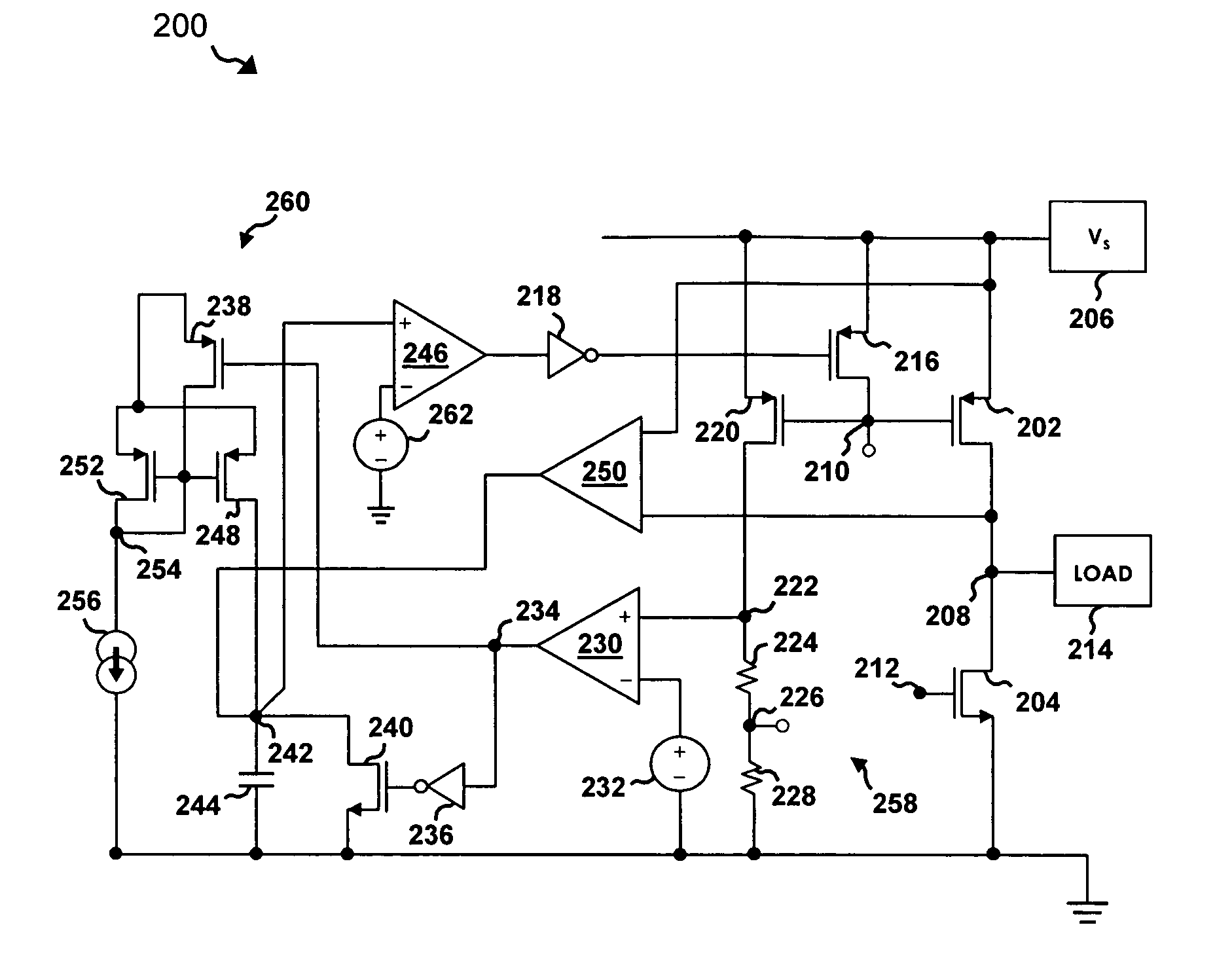
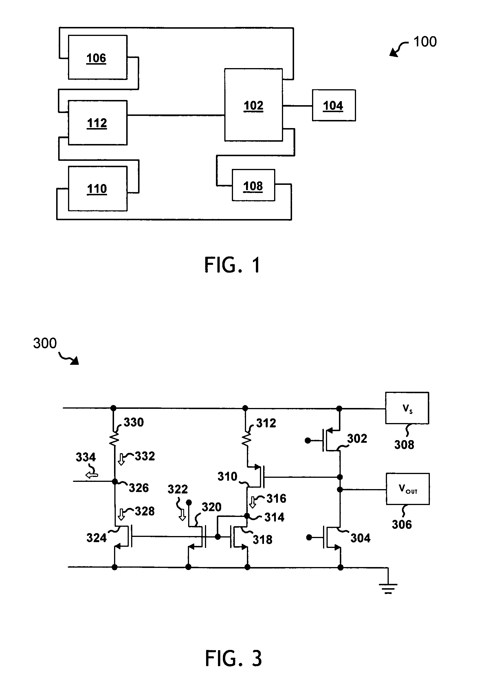
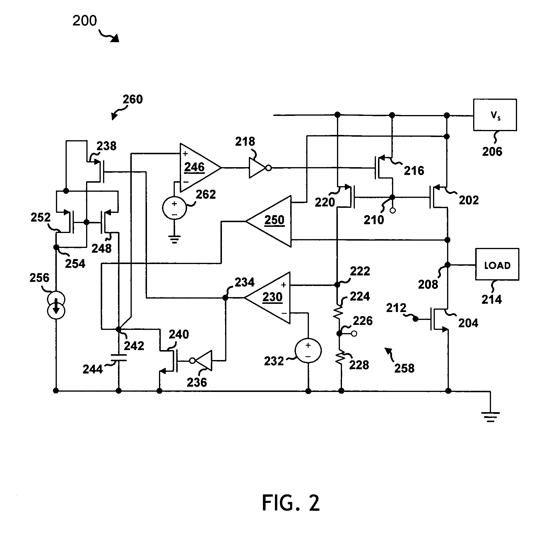
[0023]While the making and using of various embodiments of the present invention are discussed in detail below, it should be appreciated that the present invention provides many applicable inventive concepts, which can be embodied in a wide variety of specific contexts. The present invention is hereafter illustratively described primarily in conjunction with the design and operation of driver circuitry in the form an operational amplifier. Certain aspects of the present invention are further detailed in relation to design and operation of circuitry utilizing a PMOS transistor within a CMOS semiconductor process. Although described in relation to such structures, the teachings and embodiments of the present invention may be beneficially implemented with a variety of semiconductor devices or structures (e.g., NMOS transistors, low / high side driver systems). The specific embodiments discussed herein are, therefore, merely demonstrative of specific ways to make and use the invention and...


PUM


Abstract

The present invention provides a system for limiting energy levels across the output of a driver circuitry segment (100). The system provides an output structure (102) adapted to drive an output load (104). A transconductance component (106) is communicatively coupled to the output structure, and adapted to output a transconductance current that is proportional to the voltage across the output structure. A scaling component (108) is communicatively coupled to the output structure, and adapted to output a scaled current that is proportional, by some scaling factor, to the current through the output structure. A qualifying component (110) is communicatively coupled to the scaling component, and adapted to activate a trigger component (112) when the scaled current passes a first threshold. The trigger component is communicatively coupled to the qualifying component, the transconductance component, and the output structure. Responsive to activation from the qualifying component, the trigger component receives the transconductance current and accumulates charge, for an amount of time inversely proportional to the transconductance current's magnitude, and triggers shut off of the output structure when the accumulated charge passes a second threshold.

Description

TECHNICAL FIELD OF THE INVENTION[0001]The present invention relates generally to the field of semiconductor devices and, more particularly, to a versatile system of apparatus and methods for limiting energy overload across driver output circuitry.BACKGROUND OF THE INVENTION[0002]The continual demand for enhanced integrated circuit performance has resulted in, among other things, a dramatic reduction of semiconductor device geometries, and continual efforts to optimize the performance of every substructure within any semiconductor device. A number of improvements and innovations in fabrication processes, material composition, and layout of the active circuit levels of a semiconductor device have resulted in very high-density circuit designs. Increasingly dense circuit design has not only improved a number of performance characteristics, it has also increased the importance of, and attention to, semiconductor material properties and behaviors.[0003]The increased packing density of the...

Claims


Application Information

Patent Timeline
Patent Type & Authority Patents(United States)
IPC IPC(8): H03B1/00
CPCH03K17/0822H03K19/00315H03K19/0013H03K2017/0806
Inventor MACLEAN, KENNETH G.BALDWIN, DAVID J.HAGAN, TOBIN
Owner TEXAS INSTR INC
Why Eureka
Try Eureka