Signal compensation circuit and demodulating circuit with high-speed and low-speed feedback loops

a signal compensation circuit and feedback loop technology, applied in the direction of dc level restoring means or bias distorting correction, pulse technique, baseband system details, etc., can solve the problem of reducing the tolerance of run length, the inability to tolerate long run lengths, and the inability to achieve high-speed dc offset compensation

Inactive Publication Date: 2006-04-25
LAPIS SEMICON CO LTD
View PDF7 Cites 4 Cited by
  • Summary
  • Abstract
  • Description
  • Claims
  • Application Information

AI Technical Summary

Benefits of technology

[0018]The invented demodulating circuit can compensate for DC offset rapidly through the action of the high-speed compensation circuit. The time constant of the integrating circuit can also be set to tolerate DC offset variations caused by runs of identical codes, without affecting the ability for rapid DC offset compensation.
[0019]If the allowable amplitude range is expanded when the amplified signal goes outside the allowable amplitude range, then a correct digital output signal can be obtained even if in-channel noise is superimposed on a run of identical codes in the desired signal.

Problems solved by technology

Generally speaking, the capability to tolerate long run lengths conflicts with the capability for high-speed DC offset compensation.
The circuit configuration described in Document D1 is problematic in that the time needed for DC offset compensation is the total sum of the time needed for smoothing the detected signal and the absolute delay times of the channel selection filter and detector, and in that high-speed DC offset compensation is difficult if a high-order filter is used in the demodulating circuit.
The circuit configuration described in Document D2 is also problematic, in that high-speed DC offset compensation requires the time constants of the integrating circuits that detect the maximum and minimum levels of the detected signal to be decreased, which reduces the run-length tolerance.

Method used


Image

  • Signal compensation circuit and demodulating circuit with high-speed and low-speed feedback loops
  • Signal compensation circuit and demodulating circuit with high-speed and low-speed feedback loops
  • Signal compensation circuit and demodulating circuit with high-speed and low-speed feedback loops

Examples


Embodiment Construction

[0038]An embodiment of the invention will be described with reference to the attached drawings.

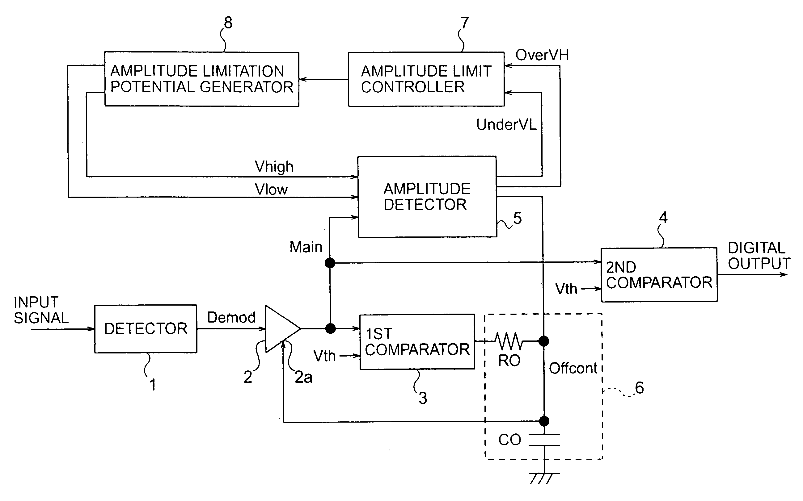
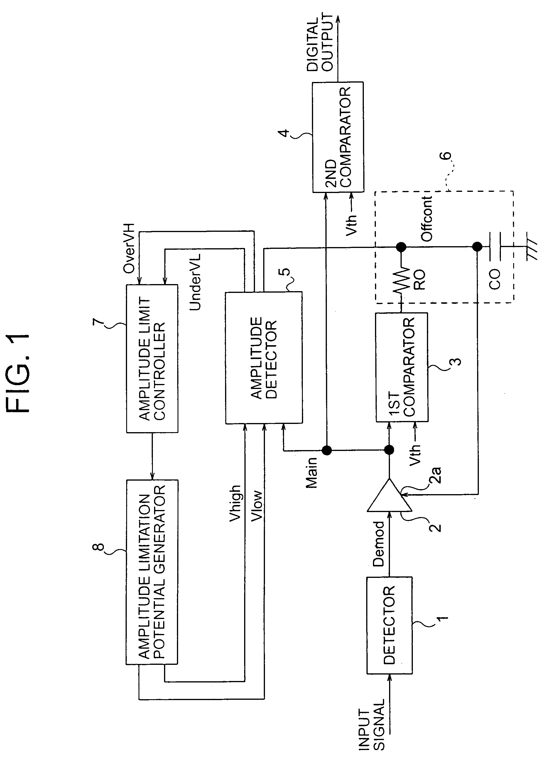
[0039]Referring to FIG. 1, the demodulating circuit in the embodiment includes a detector 1, an amplifier 2, a first comparator 3, a second comparator 4, an amplitude detector 5, an integrating circuit 6, an amplitude limit controller 7, and an amplitude limitation potential generator 8. The integrating circuit 6 includes a resistor RO and a capacitor CO. The amplifier 2, first comparator 3, amplitude detector 5, resistor RO, capacitor CO, amplitude limit controller 7, and amplitude limitation potential generator 8 constitute a signal compensation circuit embodying the invention.

[0040]The detector 1 demodulates an input signal (an FSK signal, for example), and outputs the demodulated signal (the detected signal) as an analog signal to the amplifier 2.

[0041]The amplifier 2 amplifies the demodulated analog signal to an amplitude level adequate for operation of the comparators 3 and 4, and ou...


PUM


Abstract

A signal compensation circuit compensates for direct-current offset of an input signal by amplifying the input signal with an amplifier having a variable direct-current offset. A low-speed negative feedback loop charges and discharges a capacitor in an integrating circuit according to the direct-current component of the amplified signal. A high-speed negative feedback loop charges and discharges the same capacitor at a faster rate when the amplified signal goes outside an allowable amplitude range. The capacitor potential is used to control the direct-current offset of the amplifier. The allowable amplitude range is adjusted according to the amplitude of the amplified signal. High-speed compensation can thus be combined with a tolerance for runs of identical code levels in the input signal.

Description

BACKGROUND OF THE INVENTION[0001]1. Field of the Invention[0002]The present invention relates to a signal compensation circuit and a demodulating circuit that are useful in, for example, a mobile communications receiver.[0003]2. Description of the Related Art[0004]When a signal modulated by frequency-shift keying (FSK, a common modulation method in wireless communications) is demodulated, the direct-current (DC) component of the demodulated signal (also referred to as the detected signal) may include an undesired and variable offset due to, for example, a difference between the signal frequency and the predetermined carrier frequency.[0005]U.S. Pat. No. 6,104,238 (hereinafter, Document D1) discloses a method of reducing DC potential variations in the detected output signal by varying the center frequency of, for example, a channel selection filter in a stage preceding the detector. In this method, variations in the DC offset are tracked by smoothing the detected signal and adding it...

Claims


Application Information

Patent Timeline
Patent Type & Authority Patents(United States)
IPC IPC(8): H03K3/00H03K5/13H04L27/14H03D3/00H03F3/45H04B1/16
CPCH03F3/45973H03D3/001
Inventor YOSHIDA, AKIRAHORIKAWA, AKIRAMATSUMOTO, SHUICHI
Owner LAPIS SEMICON CO LTD
Why Eureka
Try Eureka