Method for manufacturing an electron source substrate

a technology of electron source and substrate, which is applied in the manufacture of discharge tube main electrodes, electrode systems, electric discharge tube/lamps, etc., can solve the problems of image quality degradation, image quality degradation, and unsolved, and achieves low cost, high throughput, and high quality.

Inactive Publication Date: 2006-05-02
CANON KK
View PDF7 Cites 6 Cited by
  • Summary
  • Abstract
  • Description
  • Claims
  • Application Information

AI Technical Summary

Benefits of technology

[0019]The present invention has been conceived in view of the circumstances thus far described and has an object to provide a technique for manufacturing an electron source substrate of a high quality at a low cost and with a high throughput.
[0025]By thus using different kinds of ink jet devices for (1) the electrode pairs arranged at predetermined regions or at regions required to have a high positional accuracy and (2) the remaining electrode pairs, it is possible to achieve both low cost and high throughput.
[0026]Here, the phrase “different kinds” means that the ink jet devices have different performances and specifications. For the electrode pairs arranged at the regions required to have a high positional accuracy, for example, there may be used an ink jet device that has excellent performances in drop placement accuracy or drop volume accuracy. For the electrode pairs arranged near the fixed position of the spacer, for example, there may be used n ink jet device that has a nozzle arrangement different from that for the remaining electrode pairs. Here, in order to improve the production yield of the ink jet device having the special performances and specifications it is possible to reduce the number of nozzles provided on that ink jet device, as compared to the other ink jet device(s).
[0028]Because the invention uses a plurality of kinds of ink jet devices for different regions, respectively, as has been described hereinabove, an electron source substrate of a high quality can be manufactured at a low cost and with a high throughput.

Problems solved by technology

However, the following problems are left unsolved in the aforementioned manufacturing method.
As a result, the positions of the electron emission portions to be manufactured may vary, resulting in a degradation of the image quality.
If this variation occurs, especially at such a portion of the screen that displays important information, e.g., the central portion of the screen, the degradation of the image quality is easily recognized, causing a problem for the display device.
In the case of the aforementioned display device using the spacer, on the other hand, even slight positional displacement of the electron emission portions near the spacer at the time of manufacturing exerts serious influences on the electron orbits, thereby distorting the display image, so that the image quality is seriously degraded.
In this case, however, the production yield of the ink jet device itself drops so that the cost for the electron source substrate also rises disadvantageously.
For example, in case the conductive thin films are to be formed as a whole by the ink jet device having a plurality of nozzles, however, the positions of the electron emission portions cannot be individually controlled, making it difficult to form the electron source substrate of a high quality at a high throughput.

Method used


Image

  • Method for manufacturing an electron source substrate
  • Method for manufacturing an electron source substrate
  • Method for manufacturing an electron source substrate

Examples


first embodiment

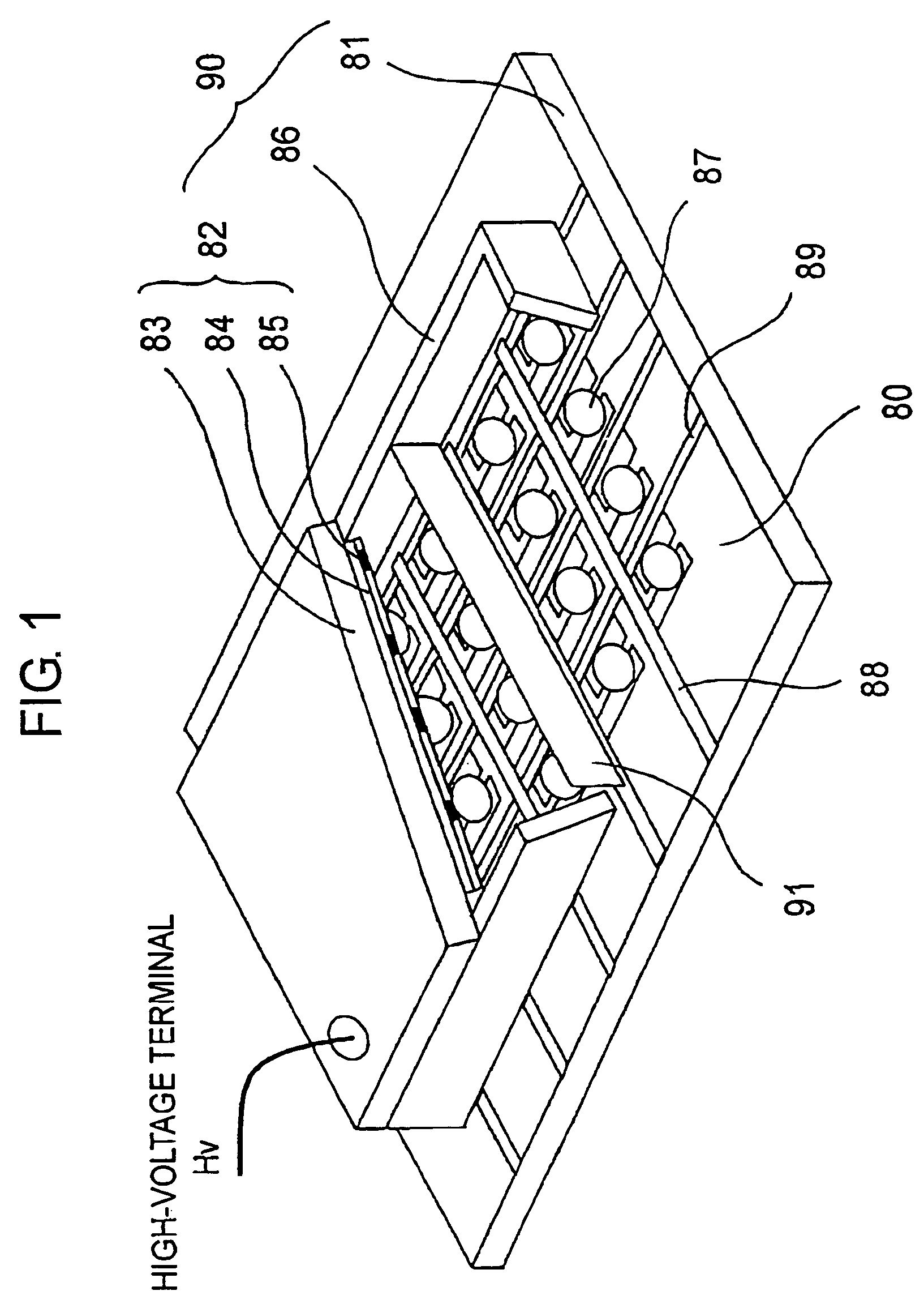
[0048]FIG. 1 is a schematic perspective view showing an image display device as an applied example of an electron source substrate according to the first embodiment of the invention.

[0049]The image display device is schematically constructed to include a rear plate 81 and a face plate 82.

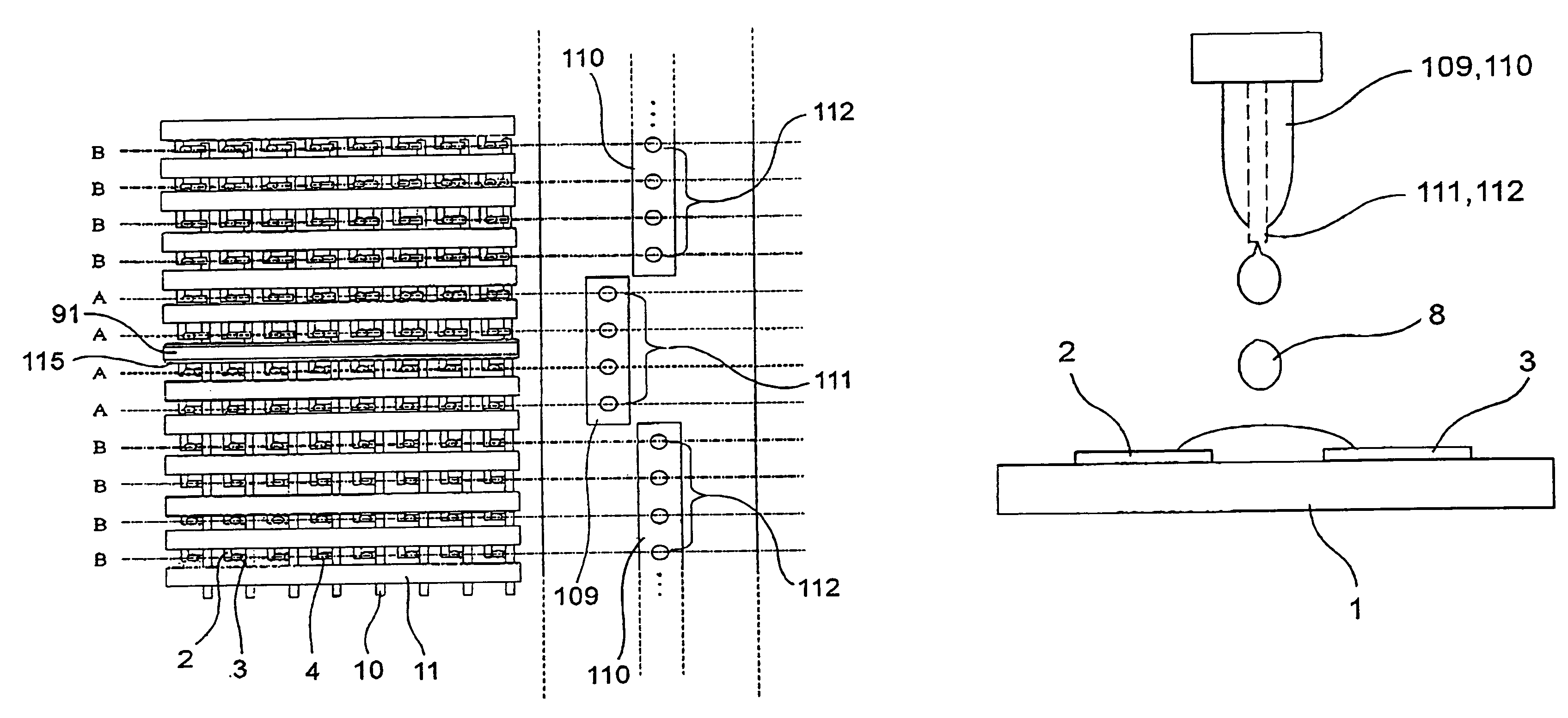
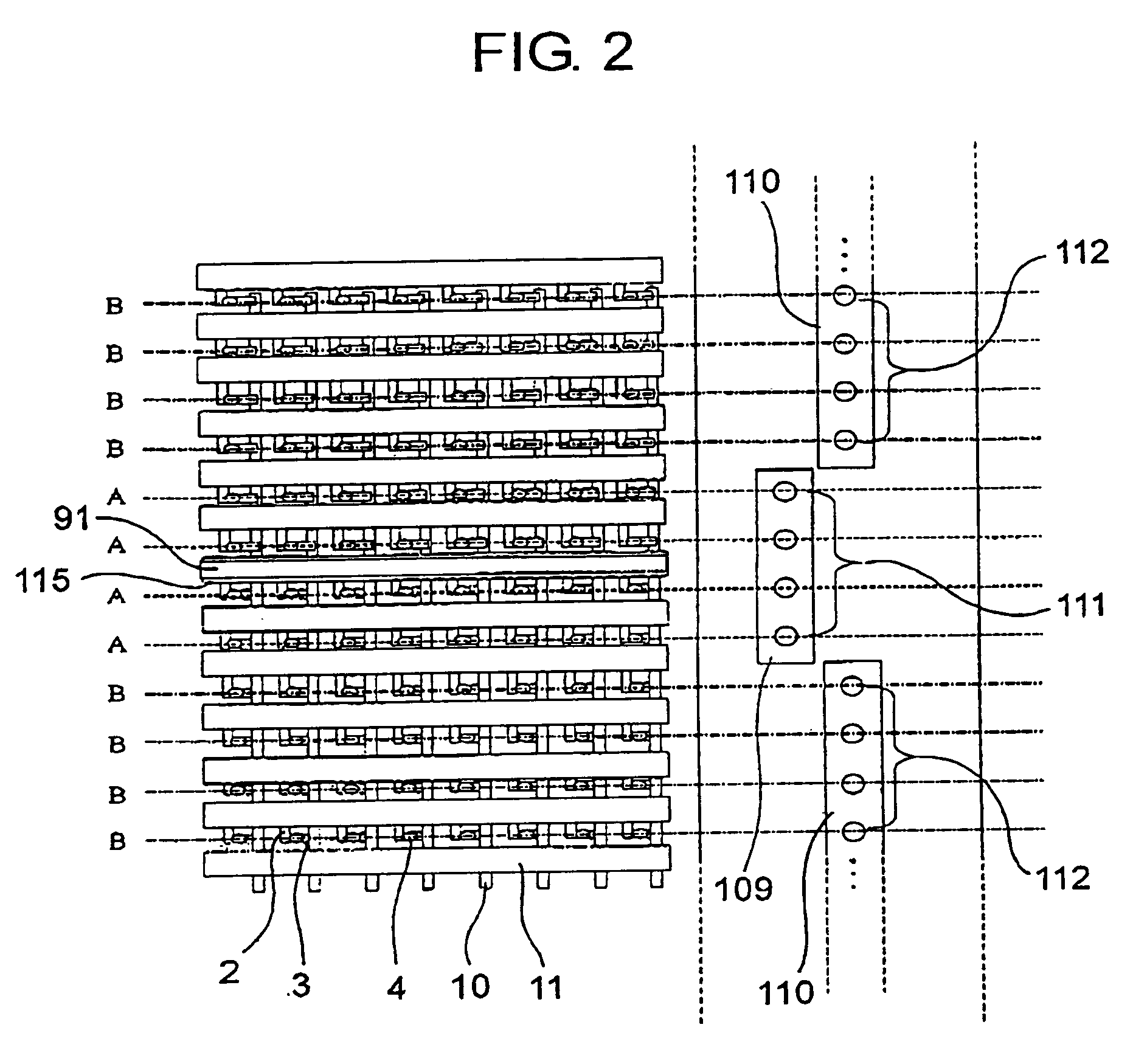
[0050]The rear plate 81 is provided with an electron source substrate 80 having a plurality of electron emission portions formed therein. This electron source substrate 80 is provided with a plurality of electron emission elements 87 arrayed two-dimensionally in the X-direction and the Y-direction, and X-direction wires 88 and Y-direction wires 89 for wiring those electron emission elements 87 in a simple matrix shape. Here in FIG. 1, only 5×4 (twenty) electron emission elements 87 are shown for simplicity of explanation. As a matter of fact, however, the electron emission elements 87 are arrayed in the order of several millions to several tens millions.

[0051]The face plate 82 is constructed such th...

second embodiment

[0094]Next, a second embodiment of the invention will be described with reference to FIG. 13.

[0095]In this embodiment, for the element electrode pairs arranged near the fixed position of the spacer, there is used an ink jet device that has a nozzle arrangement different from that used for the element electrode pairs. The remaining constructions and actions pertaining to the remaining element electrode pairs are similar to those of the first embodiment so that the detailed description of the portions having similar constructions is omitted.

[0096]As has been described, the electrons emitted from the electron emission elements on the first and second adjacent rows in the vicinity of the spacer are curved in their orbits by the influences of the spacer charge. It has been found that the curving direction approaches the spacer, and that the curvature is larger on the first adjacent row than on the second adjacent row. Considering the curvature of the electron orbits caused by the spacer ...

third embodiment

[0102]Next, a third embodiment of the invention will be described with reference to FIGS. 14 and 15.

[0103]In this embodiment, for the element electrode pairs arranged at the central portion of the screen, there is used an ink jet device of a kind different from that used for the element electrode pairs arranged at the end portions of the screen. The constructions and actions pertaining to the element electrode pairs arranged at the end portions of the screen are similar to those pertaining to the remaining element electrode portions of the first embodiment so that the detailed description of the portions having similar constructions is omitted.

[0104]The sensitivity of a human subject to the display screen is not identical for all positions on the screen. According to the experiments, as shown in FIG. 14, it has been found that the sensitivity of a subject is the highest for the region within a narrow angle of view (i.e., at the central portion of the screen) and becomes lower as the...


PUM


Abstract

A plurality of kinds of ink jet devices are used for different regions, respectively. For element electrode pairs arranged in the vicinity of the fixed position of a spacer for example, there is used an ink jet device having an excellent performance in drop placement accuracy, drop volume accuracy or the like. For the remaining element electrode pairs, there are used ink jet devices having an inferior performance. As a result, an electron source substrate of a high quality can be manufactured at a low cost and with a high throughput.

Description

BACKGROUND OF THE INVENTION[0001]1. Field of the Invention[0002]The present invention relates to a method for manufacturing an electron source substrate to be used in an electron beam device and an image forming device such as an image display device or an application of the electron beam device.[0003]2. Description of the Related Art[0004]The electron source substrate of this kind is provided with a plurality of electron emission elements constructing an electron emission portion. As the electron emission elements, there are generally known two kinds a thermal electron source and a cold cathode electron source. The cold cathode electron source is divided into a field emission element (FE element), a metal-insulator-metal element (MIM element), a surface-conduction electron-emitting element (SCE element), and so on.[0005]FIG. 16 is a diagram showing an element construction of M. Hartwell as a typical element construction of the surface-conduction electron-emitting element. In FIG. 1...

Claims


Application Information

Patent Timeline
Patent Type & Authority Patents(United States)
IPC IPC(8): H01J9/24B41J2/01H01J1/30H01J9/00H01J9/02H01L21/00
CPCH01J9/027H01J2329/00H01J2201/3165H01J9/02
Inventor MISHIMA, SEIJI
Owner CANON KK
Why Eureka
Try Eureka