Method of manufacturing a semiconductor device without oxidized copper layer

a technology of oxidized copper and semiconductors, applied in the direction of semiconductor devices, basic electric elements, electrical appliances, etc., can solve the problems of low yield rate, copper oxide layer (cuo) (i.e., natural oxide layer) formation on the copper layer, etc., and achieve the effect of eliminating

Inactive Publication Date: 2006-05-02
DONGBUANAM SEMICON
View PDF5 Cites 80 Cited by
  • Summary
  • Abstract
  • Description
  • Claims
  • Application Information

AI Technical Summary

Benefits of technology

[0020]Accordingly, the natural oxide layer can be effectively removed ...

Problems solved by technology

This technology, however, has numerous drawbacks.
A step from a surrounding portion of the connection is often enlarged; step coverage is lowered; and a short between the conductive lines is often caused which leads to low yield rates, since, after plug is formed in a contact hole or via hole of a second insulating layer, conductive line is formed on the plug.
In the conventional method of forming the conductive line and the connecting portion of the conductive line of the semiconductor device, in a case where the conductive line and the connecting portion of the conductive line are formed using Cu, as described above, there is a problem in that a copper oxide layer (CuO) (i.e., a natural oxide layer) forms on the copper layer.
In such Dual Damascene process using copper as described above, the generation of copper oxide layer cannot be avoided.
The copper oxide layer formed on ...

Method used


Image

  • Method of manufacturing a semiconductor device without oxidized copper layer
  • Method of manufacturing a semiconductor device without oxidized copper layer
  • Method of manufacturing a semiconductor device without oxidized copper layer

Examples


Embodiment Construction

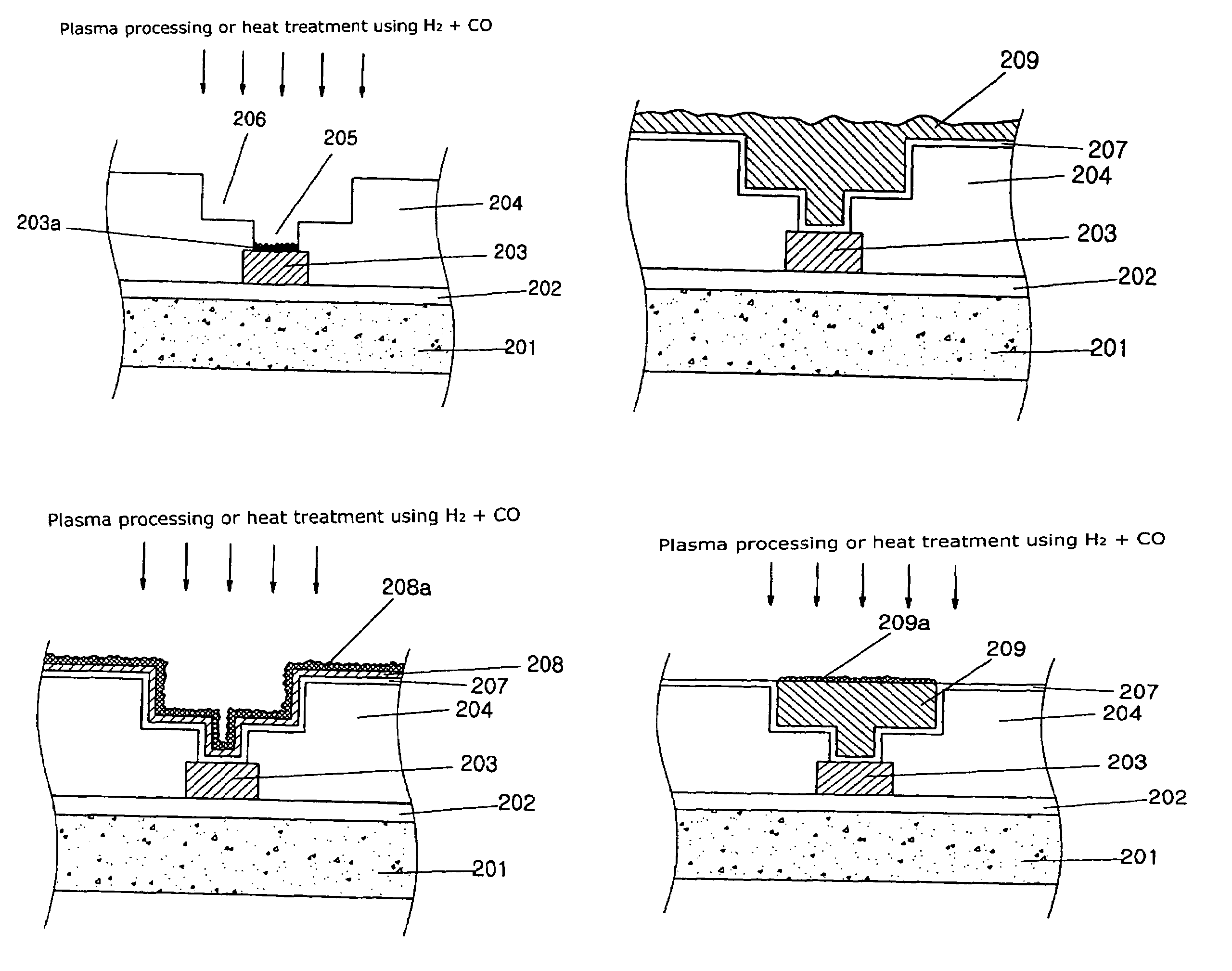
[0024]Hereinafter, a preferred embodiment of the present invention will be described with reference to FIGS. 2a to 2d, which illustrate a method of manufacturing a semiconductor device.

[0025]As shown in FIG. 2a, a first insulating layer 202 is deposited on a semiconductor substrate 201 by a chemical vapor deposition (CVD) process. Herein, the semiconductor substrate 201 can be a semiconductor substrate with an impurity region (not shown), or a lower conductive line. A lower metal layer is then formed on the first insulating layer 202. This can be performed by a sputtering method, etc. The lower metal layer is selectively patterned to form a first conductive line 203 using photolithography and etching. Herein, the lower metal layer can be composed of copper.

[0026]A second insulating layer 204 is then deposited on the first insulating layer 202 and the first conductive line 203. The second insulating layer 204 can be composed of a Tetra Ethyl OrthoSilicate (TEOS) and a Spin On Glass (...


PUM


Abstract

A semiconductor device which effectively reduces copper oxide layers on copper conductive lines is disclosed. The method includes forming a first insulating layer on a semiconductor substrate; forming a first conductive line by depositing a conductive material on the first insulating layer and selectively patterning the conductive material. A second insulating layer is deposited on top of the substrate including on the first conductive line. A via hole is formed by selectively patterning the second insulating layer to expose a certain portion of the first conductive line. A natural oxide layer is removed by plasma-processing the natural oxide layer using H2+CO gas.

Description

CROSS REFERENCE TO RELATED APPLICATIONS[0001]This application relates to and claims priority to Korean Patent Application No. 10-2002-0080216, filed on Dec. 16, 2002, the contents of which are incorporated herein by reference.BACKGROUND OF THE INVENTION[0002]1. Field of the Invention[0003]The present invention relates to a method of manufacturing a semiconductor device and, more particularly, to a method of manufacturing a semiconductor device which effectively removes copper oxide layers on copper conductive lines.[0004]2. Description of Related Art[0005]It is generally known in the art to form a connecting portion as an electric connection between devices of a semiconductor apparatus by adapting a copper conductive line. This technology, however, has numerous drawbacks. A step from a surrounding portion of the connection is often enlarged; step coverage is lowered; and a short between the conductive lines is often caused which leads to low yield rates, since, after plug is formed ...

Claims


Application Information

Patent Timeline
IPC IPC(8): H01L21/44H01L21/28H01L21/768
CPCH01L21/76814H01L21/76843H01L21/76877H01L21/76864H01L21/76873H01L21/76862H01L21/28
Inventor LEE, HAN CHOON
Owner DONGBUANAM SEMICON
Why Eureka
Try Eureka