Integrated circuit memory devices having memory cells therein that utilize phase-change materials to support non-volatile data retention

a phase-change material and integrated circuit technology, applied in the direction of semiconductor devices, electrical devices, transistors, etc., can solve the problems of less than a year for gst layer as a phase-change material layer, device data loss, and device data retention. achieve the effect of more efficient performan

Inactive Publication Date: 2006-05-02
SAMSUNG ELECTRONICS CO LTD
View PDF3 Cites 47 Cited by
  • Summary
  • Abstract
  • Description
  • Claims
  • Application Information

AI Technical Summary

Benefits of technology

[0009]Integrated circuit memory devices according to embodiments of the present invention contain memory cells that utilize phase-change materials to provide non-volatile storage. According to preferred aspects of these embodiments, operations to write cells with new data are performed more efficiently by limiting the contact area between a plate electrode and the phase-change material layer that is programmed using resistive heating. Memory cells according to embodiments of the present invention include a first electrically conductive barrier layer and a phase-change material layer pattern that extends on the first electrically conductive barrier layer. An electrically insulating layer, which extends on the phase-change material layer pattern, is used to limit the contact area to the phase-change material layer pattern so that efficient programming of the phase-change material layer pattern can be achieved. The electrically insulating layer is provided with a contact hole therein. The contact hole exposes only a relatively small portion of an upper surface of the phase-change material layer pattern. In order to protect the phase-change material layer, an electrically conductive non-phase-change material region is provided on the exposed portion of the upper surface of the phase-change material layer pattern. This material region may include a barrier region formed of the same material as the barrier layer. An electrode, such as a plate electrode, is provided on the material region. In this manner, an electrical connection can be provided between the electrode and the phase-change material layer, with the material region acting to protect the phase-change material layer from contamination.

Problems solved by technology

The volatile memory devices lose their stored data when their power supplies are interrupted, however non-volatile memory devices retain their stored data even when their power supplies are interrupted.
When this occurs, it becomes more difficult to use the GST layer as a phase change material layer.
To prevent this, the contact area between the phase-change material layer pattern and the conductive plug is typically increased, but this increase in contact area can degrade the operating characteristic of the phase-change memory cell by increasing the power required during a writing operation.

Method used


Image

  • Integrated circuit memory devices having memory cells therein that utilize phase-change materials to support non-volatile data retention
  • Integrated circuit memory devices having memory cells therein that utilize phase-change materials to support non-volatile data retention
  • Integrated circuit memory devices having memory cells therein that utilize phase-change materials to support non-volatile data retention

Examples


Embodiment Construction

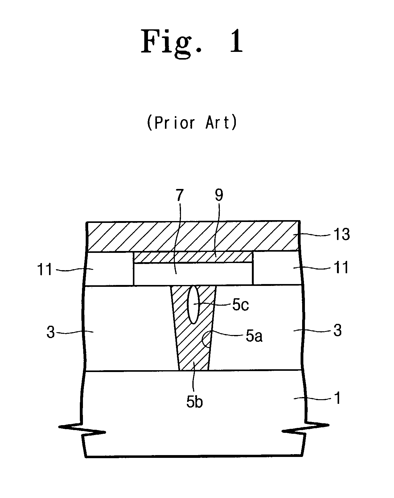
[0018]The present invention now will be described more fully herein with reference to the accompanying drawings, in which preferred embodiments of the invention are shown. This invention may, however, be embodied in many different forms and should not be construed as being limited to the embodiments set forth herein; rather, these embodiments are provided so that this disclosure will be thorough and complete, and will fully convey the scope of the invention to those skilled in the art. In the drawings, the thickness of layers and regions are exaggerated for clarity. It will also be understood that when a layer is referred to as being “on” another layer or substrate, it can be directly on the other layer or substrate, or intervening layers may also be present. Like numbers refer to like elements throughout the specification.

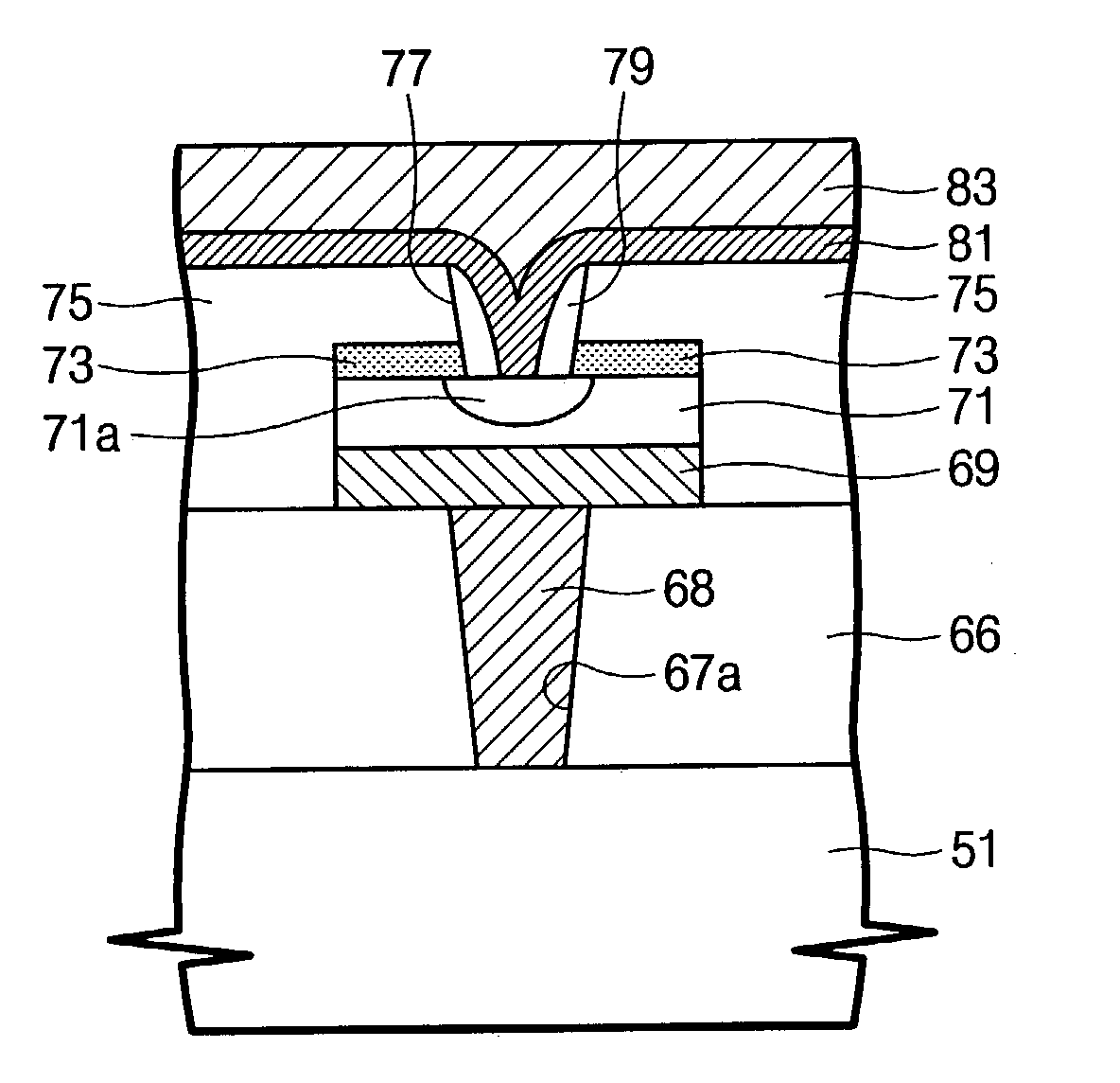
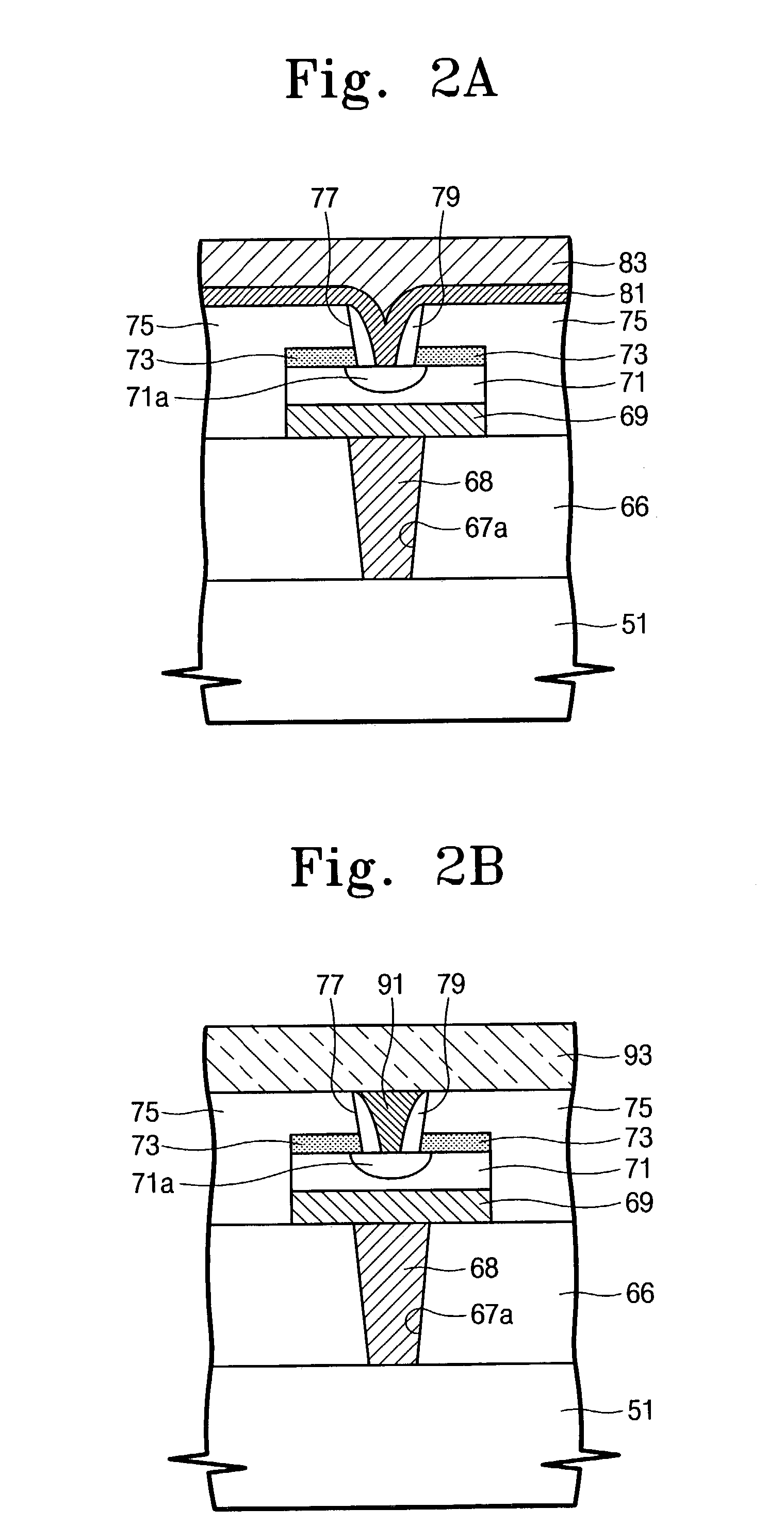
[0019]FIG. 2A is a cross-sectional view that illustrates a phase-change memory cell according to one embodiment of the present invention. Referring to FIG. 2A, a ...


PUM


Abstract

An integrated circuit memory device includes a semiconductor substrate and a first electrically insulating layer that extends on the semiconductor substrate and has a first contact hole extending therethrough. An electrically conductive plug is provided in the first contact hole. A phase-change material layer pattern is provided as a non-volatile storage medium. The phase-change material layer pattern has a bottom surface that is electrically connected to the electrically conductive plug. A second electrically insulating layer is provided on the phase-change material layer pattern. The second electrically insulating layer has a second contact hole therein. This contact hole exposes a portion of an upper surface of the phase-change material layer pattern. To improve data writing efficiency, the area of the exposed portion of the upper surface of the phase-change material layer pattern is less than a maximum cross-sectional area of the electrically conductive plug. A plate electrode is also provided. This plate electrode is electrically connected to the phase-change material layer pattern. Barrier layers may also be provided directly on the plug and directly on the exposed portion of the upper surface.

Description

REFERENCE TO PRIORITY APPLICATION[0001]This application claims priority to Korean Application No. 2002-25009, filed May 7, 2002, the disclosure of which is hereby incorporated herein by reference.FIELD OF THE INVENTION[0002]The present invention relates to integrated circuit memory devices and methods of forming same and, more particularly, to non-volatile memory devices and methods of forming non-volatile memory devices.BACKGROUND OF THE INVENTION[0003]Semiconductor memory devices can be classified into volatile memory devices and non-volatile memory devices. The volatile memory devices lose their stored data when their power supplies are interrupted, however non-volatile memory devices retain their stored data even when their power supplies are interrupted. Thus, non-volatile memory devices are widely used in memory cards, mobile telecommunication systems and other devices that are susceptible to power interruption.[0004]Non-volatile memory devices typically employ flash memory ce...

Claims


Application Information

Patent Timeline
Patent Type & Authority Patents(United States)
IPC IPC(8): H01L29/76H01L27/115H01L27/24H01L29/68H01L45/00
CPCH01L29/685H01L45/06H01L27/2436H01L45/126H01L45/144H01L45/1233H10B63/30H10N70/231H10N70/826H10N70/8413H10N70/8828H10B69/00
Inventor HORII, HIDEKI
Owner SAMSUNG ELECTRONICS CO LTD
Why Eureka
Try Eureka