Check patentability & draft patents in minutes with Patsnap Eureka AI!

Semiconductor device

a technology of semiconductor devices and phase change memory arrays, applied in static storage, digital storage, instruments, etc., can solve the problems of difficult high-speed read, difficult reduction of ferroelectric capacitor area and therefore cell area, and inability to meet the operational specifications expected for ordinary sram chips. achieve the effect of reliably operating in a short operation cycle tim

Inactive Publication Date: 2006-05-02
HITACHI LTD
View PDF4 Cites 36 Cited by
  • Summary
  • Abstract
  • Description
  • Claims
  • Application Information

AI Technical Summary

Benefits of technology

[0009]Accordingly, it is an object of the present invention to implement a highly integrated high-speed non-volatile phase change memory capable of operating reliably in a short operation cycle time.

Problems solved by technology

However, it is difficult to reduce the area of the ferroelectric capacitor in FeRAM and therefore the area of the cell.
MRAM has also a drawback that high-speed read is difficult since the magnitude of the readout signal is small due to the small change ratio of the magnetoresistance.
Merely replacing the internal memory array of a SRAM chip by a phase change memory array cannot conform to the operational specifications expected for ordinary SRAM chips.
After the resistivity-raising write operation is done, a large amount of time is also required to settle the state of the phase change resistor before the subsequent read access is done to the same memory cell.
That is, it is difficult to raise the access speed to the level of low power SRAM chips.

Method used


Image

  • Semiconductor device
  • Semiconductor device
  • Semiconductor device

Examples


first embodiment

(First Embodiment)

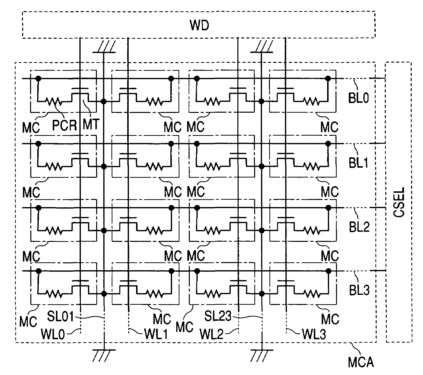
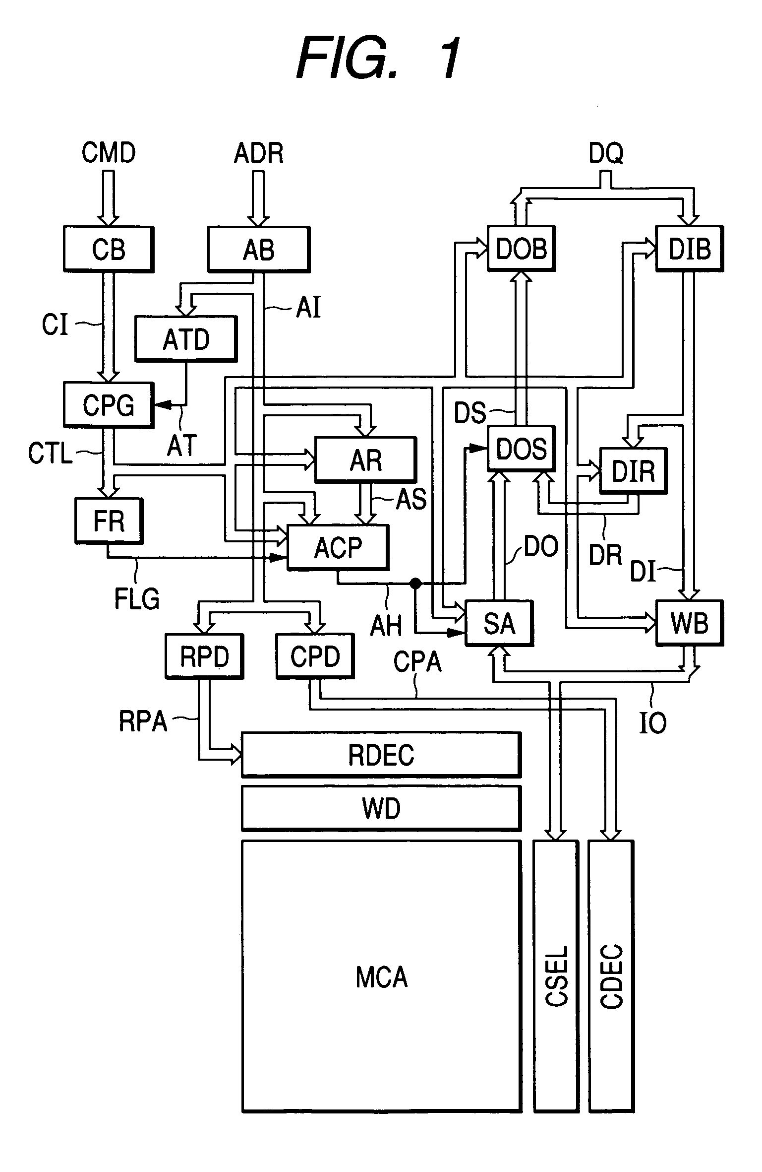
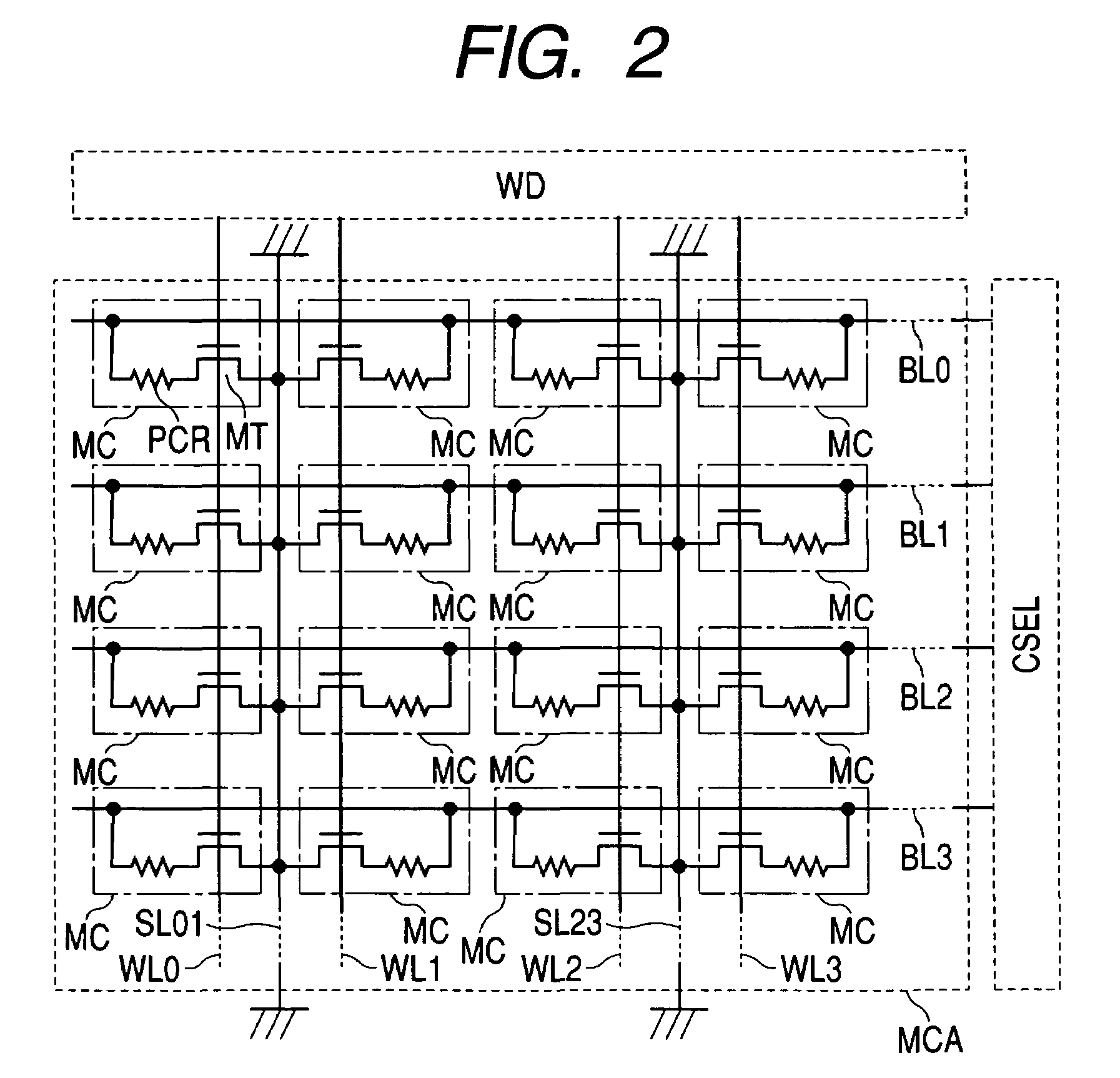
[0030]FIG. 1 is a block diagram of a key portion of an asynchronous phase change memory configured in accordance with the present invention. Generally, in an asynchronous phase change memory, an operation is performed depending on the state of the command signal when an address transition is detected, while not restrictive. The asynchronous phase change memory of the present invention, shown there, is characterized in that it has a write data register DIR, an output data selector DOS, a write address register AR, an address comparator ACP and a flag register FR. This asynchronous phase change memory also has a command buffer CB, a control signal generator CPG, an address buffer AB, an address transition detector ATD, a row predecoder RPD, a column predecoder CPD, an input buffer DIB, an output buffer DOB, a sense amplifier block SA and a write buffer block WB. Further, a memory cell array MCA is formed with a row decoder RDEC, a word driver WD, a column decoder CDE...

second embodiment

(Second Embodiment)

[0047]FIG. 9 is a block diagram of a key portion of a synchronous phase change memory configured in accordance with the present invention. Generally, a synchronous phase change memory takes in a command and address and performs an operation based on an external clock signal. As with the embodiment of an asynchronous phase change memory, shown in FIG. 1, this synchronous phase change memory of the present invention, shown in FIG. 9, includes a write data register DIR, an output data selector DOS, a write address register AR, an address comparator ACP and a flag register FR. It also includes a clock buffer CKB, a command buffer CB, a command decoder CD, an address buffer AB, a row predecoder RPD, a column predecoder CPD, an input buffer DIB, an output buffer DOB, a sense amplifier block SA and a write buffer block WB. Further, a memory cell array MCA is formed with a row decoder RDEC, a word driver WD, a column decoder CDEC and a column selector CSEL. The memory cel...

third embodiment

(Third Embodiment)

[0056]FIG. 12 is a block diagram of another example of an asynchronous phase change memory configured in accordance with the present invention. It is characterized in that a first write data register DIR1 and a second write data register DIR2 are provided to form a two-stage write data register and likewise a first write address register AR1 and a second write address register AR2 form a two-stage write address register. An address comparator AC2 compares the internal address AI with the first retained write address AS1 and second retained write address AS2 and outputs an address hit signal AH2 indicating whether the internal address AI agrees with them. Controlled by the address hit signal AH2, an output data selector DS3 selects output data DS from the readout data DO, first retained write data DR1 and second retained write data DR2 and outputs the output data DS. If the internal address AI agrees with the first retained write address AS1, the first retained writ...


PUM


Abstract

A phase change memory is provided with a write data register, an output data selector, a write address register, an address comparator and a flag register. Write data is not only written into a memory cell but also retained by the write data register until the next write cycle. If a read access occurs to that address before the next write cycle, data is read out from the register without reading the data from the memory cell array. Without elongating the cycle time, it is possible not only to use long time to write data into a memory cell therein but also to make longer the interval between the time when a write operation is done and the time when the subsequent read operation is made from that memory cell. As a result, data can be written reliably.

Description

BACKGROUND OF THE INVENTION[0001]1. Field of the Invention[0002]The present invention relates to semiconductor devices and, in particular, to a semiconductor device containing a high-speed non-volatile memory which stores information in memory cells using phase change resistors.[0003]2. Description of the Related Art[0004]Aimed at a high-speed and highly integrated non-volatile memory, the development of phase change memories is now in progress as described in “2002 IEEE International Solid-State Circuits Conference, Digest of Technical Papers, pp. 202–203”. In the phase change memory, information is stored by utilizing a phase change material called a chalcogenide material which changes its resistivity depending on the state. Write operations to a phase change resistor are done by supplying a current thereto so that the resistor is heated to change the state. Lowering the resistivity, called a set operation, is done by keeping the resistor at relatively low temperature for enough l...

Claims


Application Information

Patent Timeline
Patent Type & Authority Patents(United States)
IPC IPC(8): G11C7/00G11C13/00G11C16/02
CPCG11C8/06G11C8/10G11C13/0069G11C13/0004G11C2213/79
Inventor SAKATA, TAKESHIOSADA, KENICHITAKEMURA, RIICHIROMATSUOKA, HIDEYUKI
Owner HITACHI LTD
Features
  • R&D
  • Intellectual Property
  • Life Sciences
  • Materials
  • Tech Scout
  • Unparalleled Data Quality
  • Higher Quality Content
  • 60% Fewer Hallucinations
Learn More