Supercharge Your Innovation With Domain-Expert AI Agents!

Package substrate and a flip chip mounted semiconductor device

a semiconductor device and substrate technology, applied in the direction of printed circuit stress/warp reduction, high frequency circuit adaptation, printed circuit aspects, etc., can solve the problem of mainly affecting the yield of conventional flip chip mounted semiconductor devices

Inactive Publication Date: 2006-05-09
KK TOSHIBA
View PDF7 Cites 9 Cited by
  • Summary
  • Abstract
  • Description
  • Claims
  • Application Information

AI Technical Summary

Benefits of technology

The present invention provides a package substrate and a semiconductor device with a multi-level structure that overcomes issues in the related art. The package substrate has a plurality of perforations on its top and bottom surfaces, and a built-up wiring layer implementing the multi-level structure is disposed on both surfaces. The semiconductor chip mounting region is provided on the top or bottom surface of the substrate. The semiconductor device also includes a flip chip connection bump and underfill resin to seal the gap between the package substrate and the semiconductor chip. The technical effects of this invention include improved signal integrity, reduced power consumption, and enhanced reliability.

Problems solved by technology

It has been verified that decreases in the yield of conventional flip chip mounted semiconductor devices are mainly caused by damage due to the difference in thermal expansion between a semiconductor chip and the package substrate.

Method used


Image

  • Package substrate and a flip chip mounted semiconductor device
  • Package substrate and a flip chip mounted semiconductor device
  • Package substrate and a flip chip mounted semiconductor device

Examples


first embodiment

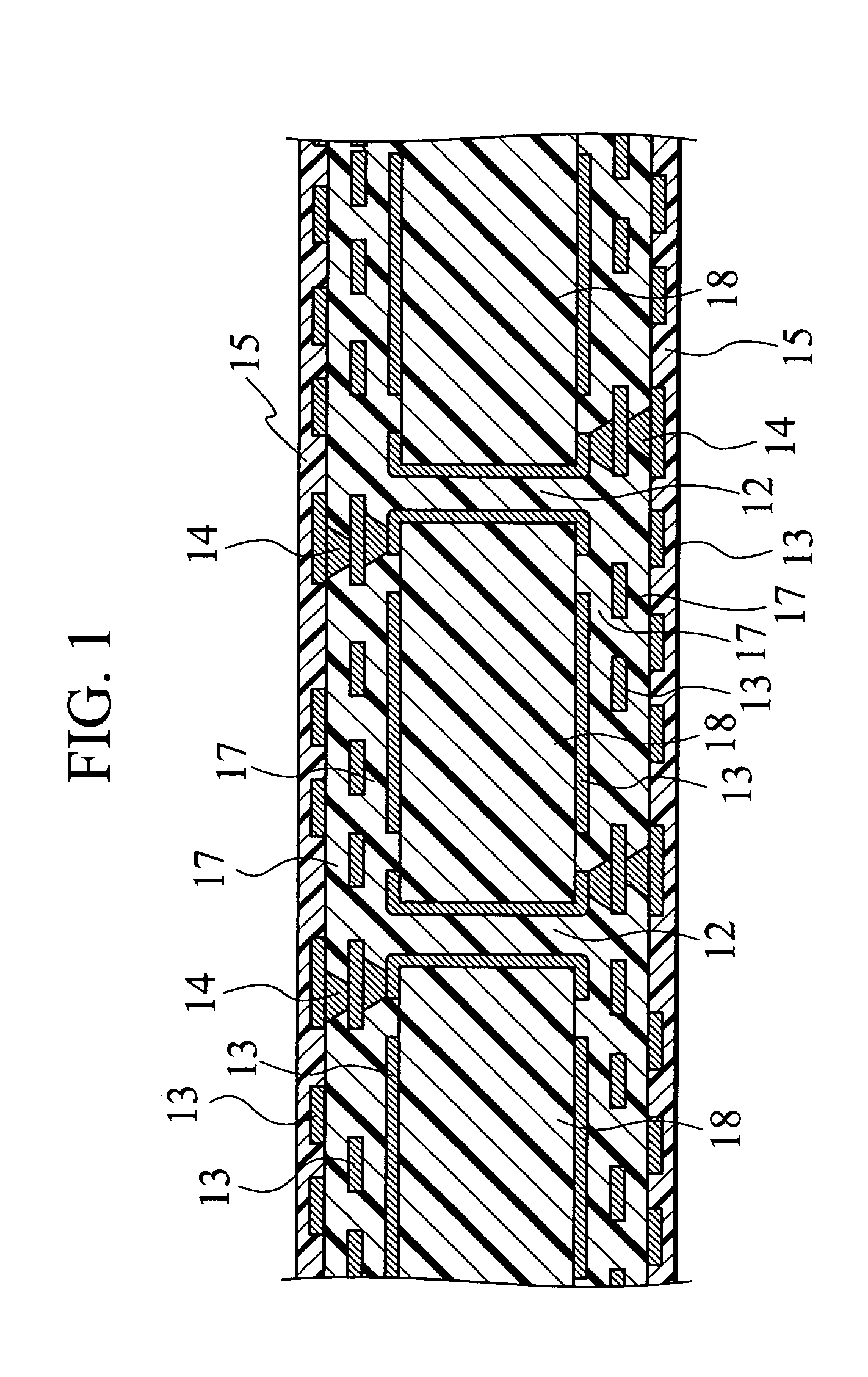
[0039]FIG. 4 is a schematic cross-sectional structural diagram showing the detailed structure of a package substrate used in a flip chip mounted semiconductor device according to a first embodiment of the present invention. The package substrate 9 according to the first embodiment of the present invention and used in a flip chip mounted semiconductor device encompasses, as shown in the cross-sectional enlarged view of FIG. 4; a metal plate core 10; perforations 11, which open to the metal plate core 10; a via 12, which is formed inside of a perforation 11; micro metal wiring 13; a micro via 14; and solder resist 15, which is formed on both the surface and undersurface of the package substrate 9. The package substrate 9 uses the metal plate core 10 as its core, and on both the surface and undersurface of this core, multiple wiring layers of micro metal wiring 13 are separated by intermediate insulation layers 17 of built-up resin. A plurality of perforations 11 are formed in the meta...

second embodiment

[0043]FIG. 5 is a schematic cross-sectional structural diagram of a flip chip mounted semiconductor device according to a second embodiment of the present invention. The flip chip mounted semiconductor device according to the second embodiment of the present invention encompasses, as shown in the illustrative cross-sectional structure of FIG. 5, a package substrate 9; a semiconductor package 1, which is connected with the package substrate 9 via flip chip connection bumps 3; underfill resin 4, which protects the connection portion between the package substrate 9 and the semiconductor package 1; and BGA balls 5, which are formed on the surface of the package substrate 9. In FIG. 5, the internal structure of package substrate 9 is shown schematically. The detailed structure of package substrate 9 is as shown in FIG. 4.

modified example 1

OF THE SECOND EMBODIMENT

[0044]FIG. 6 is a schematic cross-sectional structural diagram of a flip chip mounted semiconductor device according to a modified example 1 of the second embodiment of the present invention.

[0045]The flip chip mounted semiconductor device according to the modified example 1 of the second embodiment of the present invention encompasses, as shown in the illustrative cross-sectional structure of FIG. 6, a package substrate 9; a semiconductor package 1, which is connected with the package substrate 9 via flip chip connection bumps 3; underfill resin 4, which protects the connection portion between the package substrate 9 and the semiconductor package 1; and BGA balls 5, which are formed on the undersurface of the package substrate 9. In FIG. 6, the internal structure of package substrate 9 is shown schematically. The detailed structure of package substrate 9 is as shown in FIG. 4.

[0046]FIG. 7 is a schematic cross-sectional structural diagram showing the detailed...


PUM


Abstract

The present invention provides a package substrate which comprises a substrate defined by top and bottom surfaces and having a plurality of perforations; a resin insulation layer configured to implement a multi-level structure disposed on both surfaces of the substrate; a built-up wiring layer implementing the multi-level structure disposed on the resin insulation layer on both surfaces of the substrate; and a semiconductor chip mounting region provided on the top or the bottom surface of the substrate; wherein, a perforation exists on any straight line connecting from the center of the substrate to an arbitrary point on a periphery of the substrate.

Description

CROSS REFERENCE TO RELATED APPLICATIONS[0001]This application is based upon and claims the benefit of priority from prior Japanese Patent Application P2003-045018 filed on Feb. 21, 2003; the entire contents of which are incorporated herein by reference.BACKGROUND OF THE INVENTION[0002]1. Field of the Invention[0003]The present invention relates to semiconductor packaging. In particular, it is related to a package substrate and a flip chip mounted semiconductor device.[0004]2. Description of the Related Art[0005]Conventionally, a flip chip mounted semiconductor package includes either a ceramic substrate or resin substrate, which is used as a package substrate for wiring to mount a semiconductor chip. A semiconductor chip is connected to the package substrate via flip chip connection bumps made from soldering balls, and in order to protect that connection area, thermosetting resin, which is called underfill resin, is filled thereto. On the surface of the package substrate there are f...

Claims


Application Information

Patent Timeline
Patent Type & Authority Patents(United States)
IPC IPC(8): H01L23/12H01L21/56H01L23/14H01L23/498H05K1/02H05K1/05H05K3/44H05K3/46
CPCH01L23/49816H01L23/49822H05K1/0224H05K3/4608H01L24/32H01L21/563H01L2224/16225H01L2224/32225H01L2224/48091H01L2224/48227H01L2224/73253H01L2224/73265H01L2924/01004H01L2924/01005H01L2924/01013H01L2924/01025H01L2924/01029H01L2924/01033H01L2924/01074H01L2924/01078H01L2924/01082H01L2924/09701H01L2924/15311H01L2924/1532H01L2924/19043H05K1/0253H05K1/0271H05K1/056H05K3/445H05K2201/09309H05K2201/09536H05K2201/09609H05K2201/09681H01L24/48H01L2924/01006H01L2924/01019H01L2924/01087H01L2924/0133H01L2224/73204H01L2924/00014H01L2924/01026H01L2924/01028H01L2924/00H01L2924/3512H01L2924/00012H01L2924/15787H01L24/73H01L2224/05599H01L2224/45099H01L2224/85399H01L2924/3511H01L2224/45015H01L2924/207
Inventor SUGIZAKI, YOSHIAKIIKEBE, HIROSHI
Owner KK TOSHIBA
Features
  • R&D
  • Intellectual Property
  • Life Sciences
  • Materials
  • Tech Scout
  • Unparalleled Data Quality
  • Higher Quality Content
  • 60% Fewer Hallucinations
Learn More