Substrate brush scrubbing and proximity cleaning-drying sequence using compatible chemistries, and method, apparatus, and system for implementing the same

a technology of proximity cleaning and scrubbing sequence, applied in the direction of cleaning using liquids, household cleaners, tableware washing/rinsing machines, etc., can solve the problems of affecting the performance of integrated circuit devices, certain shortcomings, and inability to adequately clean and process the backside of wafers

Inactive Publication Date: 2006-05-16
LAM RES CORP
View PDF66 Cites 11 Cited by
  • Summary
  • Abstract
  • Description
  • Claims
  • Application Information

AI Technical Summary

Benefits of technology

[0017]The advantages of the present invention are numerous. Most notably, in contrast to the prior art wherein incompatible chemistries such as SC1 and HF are used to clean wafer backside and front side, respectively, in the embodiments of the present invention, compatible chemistries are used to clean and / or dry the wafer front side and backside. Another advantage is that by using compatible chemistries to clean wafer front side and backside, fluid handling arrangements in the brush scrubbing and proximity cleaning preparation system is simplified. Still another advantage of the present invention is that by implementing compatible chemistries to brush scrub and proximity clean and / or dry wafer surfaces, the scrubbing and proximity cleaning and / or drying chamber can be free of cross contamination. This is beneficial, as by not using incompatible chemistries, the footprint of the apparatus is also reduced. Yet another advantage is that the embodiments of the present invention simplify handling of the compatible chemistries within the apparatus thus reducing mechanical cost associated with using separate flow handling components and waste treatment units for each chemistry.

Problems solved by technology

Particulate contaminants should be removed from wafer surfaces as the existence of such contaminants can have detrimental effects on the performance of integrated circuit devices.
Cleaning the wafer front sides (i.e., the active side or top surface) has traditionally been given a higher priority in typical wafer cleaning systems and processes because deleterious defects may be caused in the processing of the wafers.
However, as wafer sizes have increased and / or feature sizes have decreased, certain shortcomings have been associated with the failure to adequately and properly clean and process wafer backsides (i.e., non-active side).
One drawback of having contaminant particulates on wafer backside is particulate contaminant migration from the wafer backside to the wafer front side.
Furthermore, the backside contaminants can undesirably migrate from one process tools or steps thus contaminating subsequent processes.
When performing the brush scrubbing, however, undesirably, the cleaning fluid SC1 can in some cases be sprayed onto the wafer front side.
As a direct result, not only the footprint of the wafer processing system is unnecessarily increased but also the system chemical handling arrangements can become very complicated.

Method used


Image

  • Substrate brush scrubbing and proximity cleaning-drying sequence using compatible chemistries, and method, apparatus, and system for implementing the same
  • Substrate brush scrubbing and proximity cleaning-drying sequence using compatible chemistries, and method, apparatus, and system for implementing the same
  • Substrate brush scrubbing and proximity cleaning-drying sequence using compatible chemistries, and method, apparatus, and system for implementing the same

Examples


Embodiment Construction

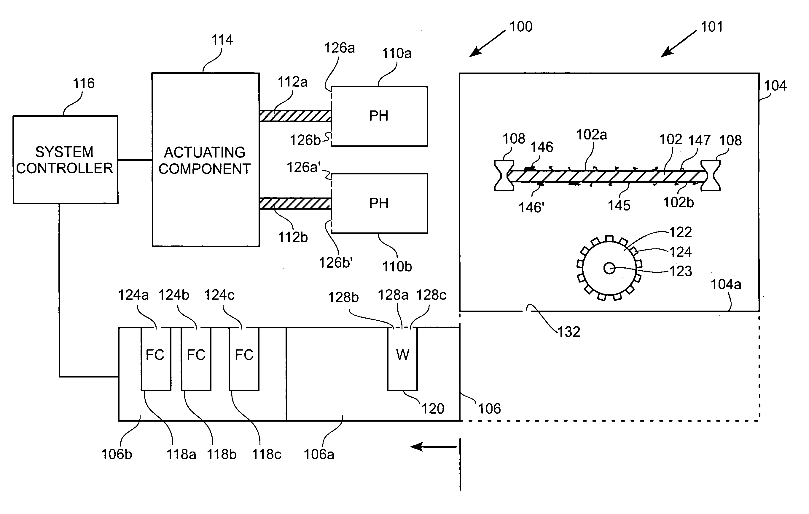
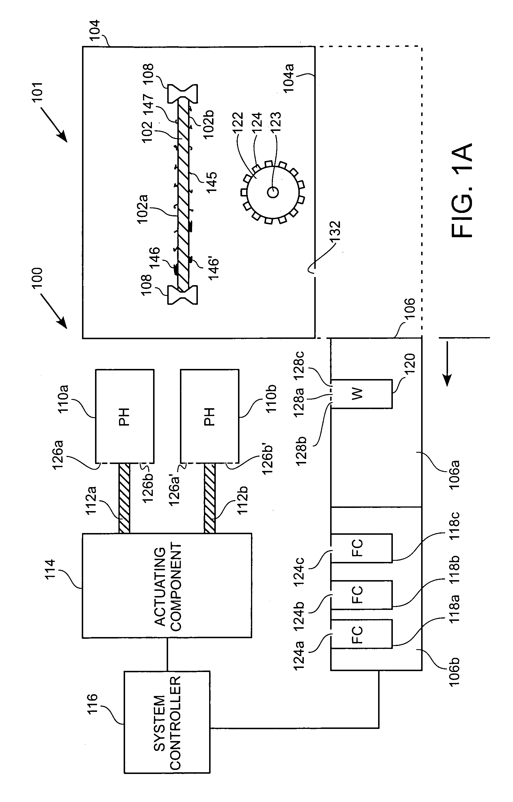
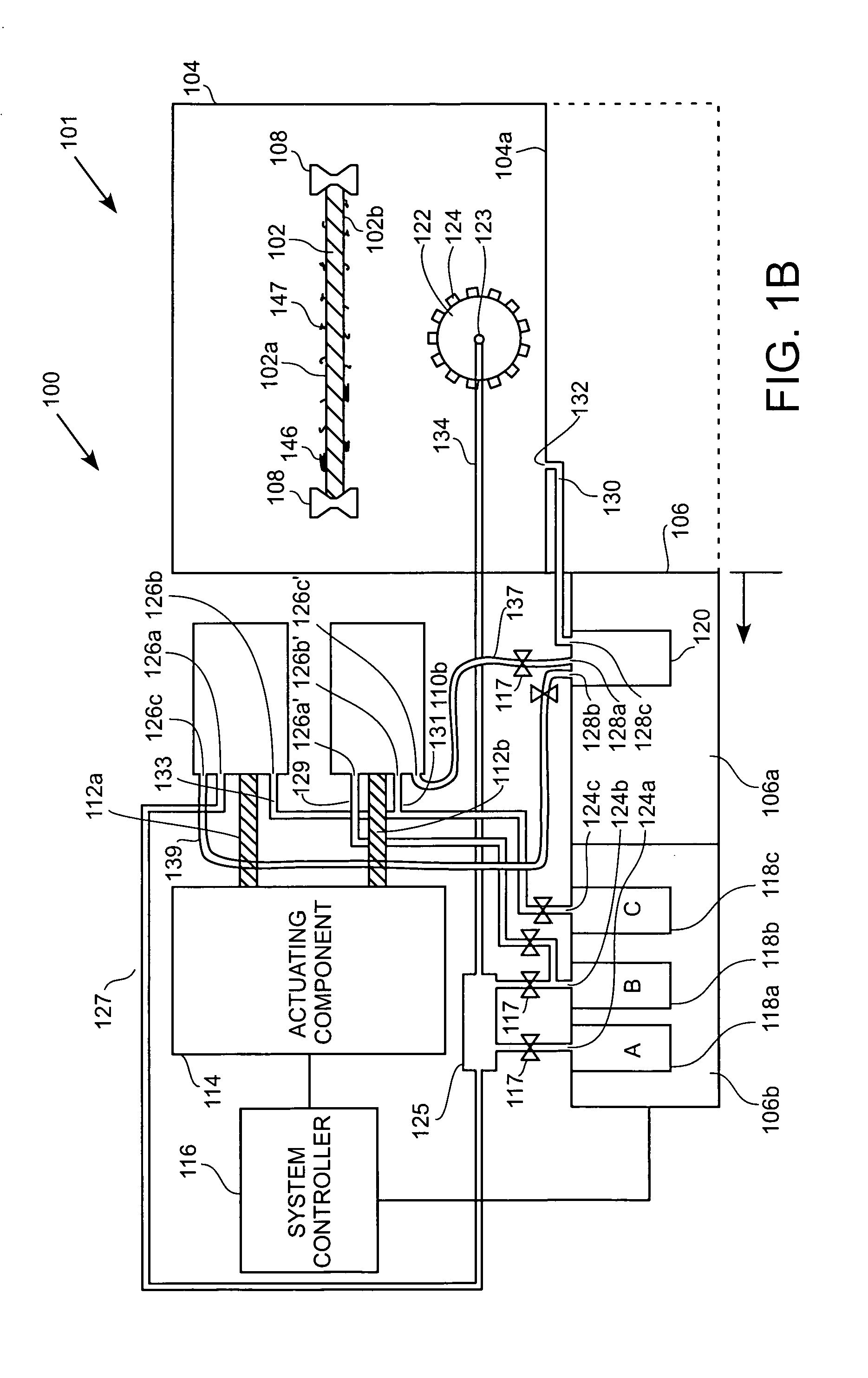
[0034]An invention capable of simplifying fluid handling arrangements and improving substrate throughput by minimizing cross contamination resulting from implementing incompatible chemistries is provided. In one embodiment, a substrate is prepared by performing a brush scrubbing operation on a substrate backside using a brush chemistry followed by proximity cleaning and / or drying of the substrate front side and backside using chemistries compatible with the brush scrubbing chemistry. In one example, a front proximity head and a back proximity head are used to clean and / or dry substrate front side and backside substantially simultaneously, using a front and a back meniscus, respectively. The front and back meniscus, as disclosed in U.S. patent application Ser. No. 10 / 261,839, filed on Sep. 30, 2002, and entitled “METHOD AND APPARATUS FOR DRYING SEMICONDUCTOR WAFER SURFACES USING A PLURALITY OF INLETS AND OUTLETS HELD IN CLOSE PROXIMITY TO THE WAFER SURFACES,” is incorporated herein b...


PUM


Abstract

A method for cleaning and drying a front and a back surface of a substrate is provided. The method includes brush scrubbing the back surface of the substrate using a brush scrubbing fluid chemistry. The method further includes applying a front meniscus onto the front surface of the substrate upon completing the brush scrubbing of the back surface. The front meniscus includes a front cleaning chemistry that is chemically compatible with the brush scrubbing fluid chemistry.

Description

CROSS-REFERENCE TO RELATED APPLICATIONS[0001]This application is a continuation-in-part of U.S. patent application Ser. No. 10 / 261,839, filed on Sep. 30, 2002, and entitled “METHOD AND APPARATUS FOR DRYING SEMICONDUCTOR WAFER SURFACES USING A PLURALITY OF INLETS AND OUTLETS HELD IN CLOSE PROXIMITY TO THE WAFER SURFACES,” from which priority under 35 U.S.C. § 120 is claimed.BACKGROUND[0002]1. Field of the Invention[0003]The present invention relates generally to substrate cleaning and drying and, more particularly, to systems, apparatuses, and methods for improving semiconductor substrate cleaning and / or drying by reducing contamination of substrate surfaces.[0004]2. Description of the Related Art[0005]The fabrication of semiconductor devices involves numerous processing operations. These operations include, for example, dopant implants, gate oxide generation, inter-metal oxide depositions, metallization depositions, photolithography patterning, etching operations, chemical mechanica...

Claims


Application Information

Patent Timeline
Patent Type & Authority Patents(United States)
IPC IPC(8): B08B7/04H01L21/00
CPCH01L21/67028H01L21/67051H01L21/67046Y10S134/902
Inventor RAVKIN, MICHAELDE LARIOS, JOHN M.
Owner LAM RES CORP
Why Eureka
Try Eureka