

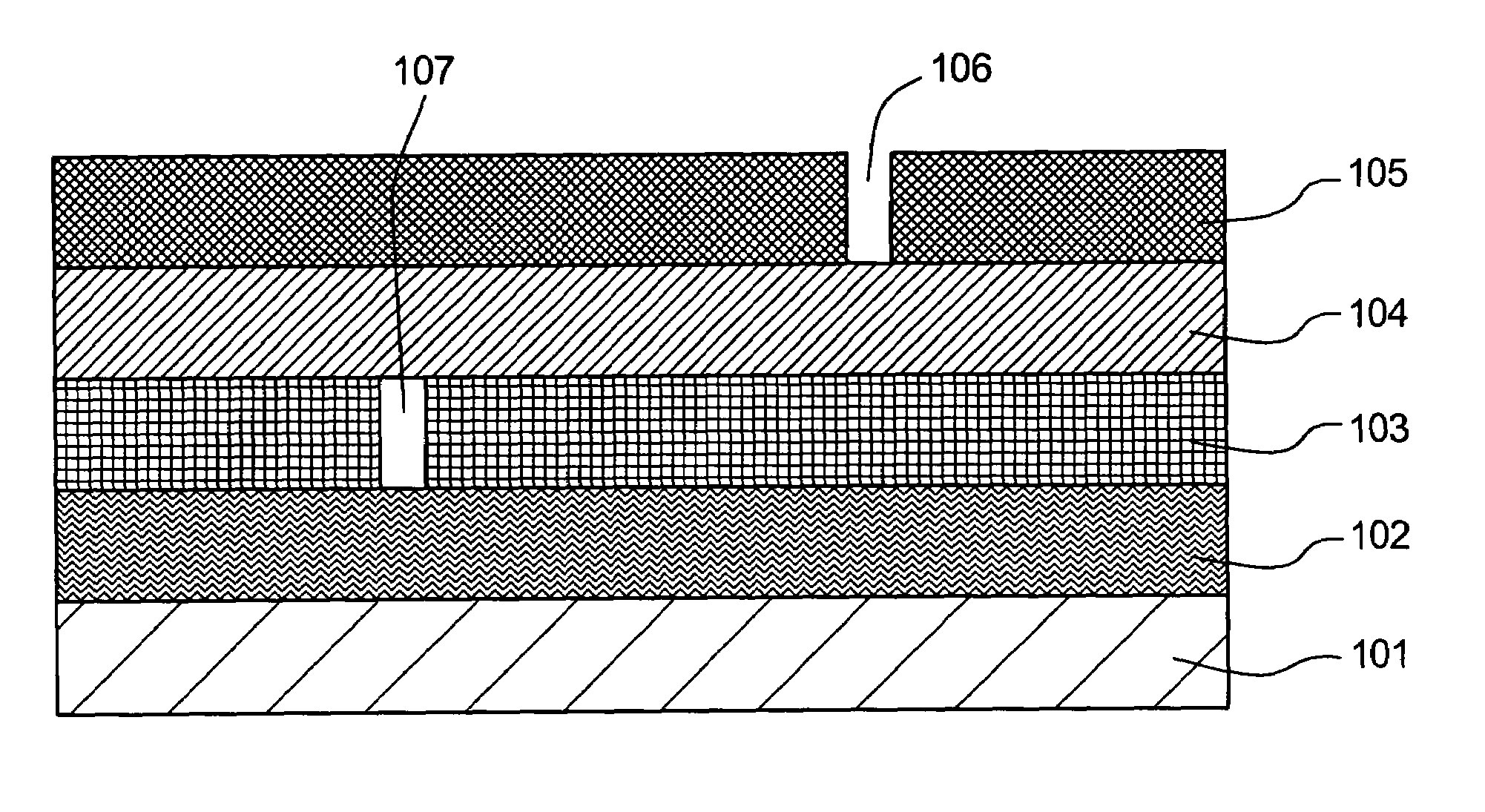
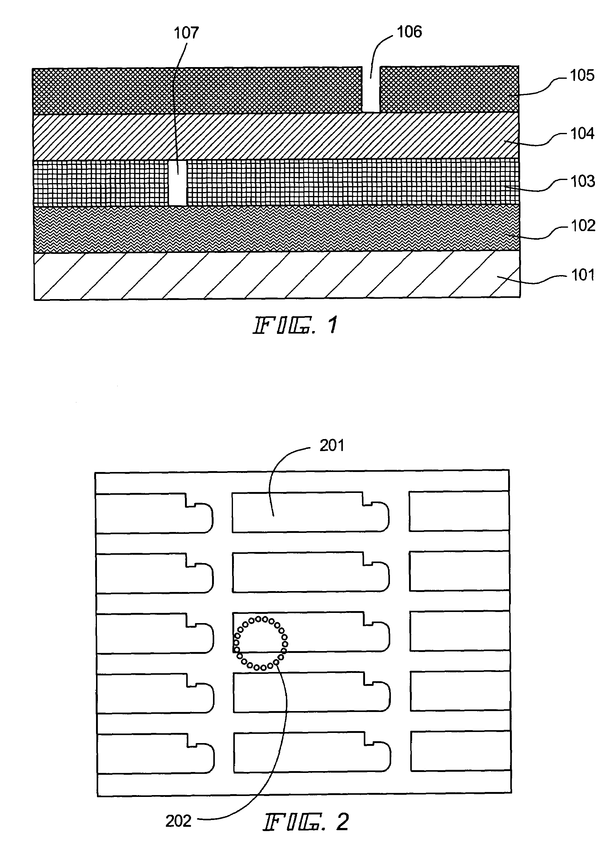
Light-emitting device having electrode formed by laminate of at least first inorganic film, organic film, and second inorganic film and method for manufacturing the same
a light-emitting device and laminate technology, which is applied in the direction of organic semiconductor devices, discharge tubes/lamp details, discharge tubes luminescnet screens, etc., can solve the problems of unstable electrodes, damage to light-emitting elements, and potential for electrical shock, so as to achieve high-reliability light-emitting devices
- Summary
- Abstract
- Description
- Claims
- Application Information
AI Technical Summary
Benefits of technology
Problems solved by technology
Method used
Image

Examples
embodiment mode 1
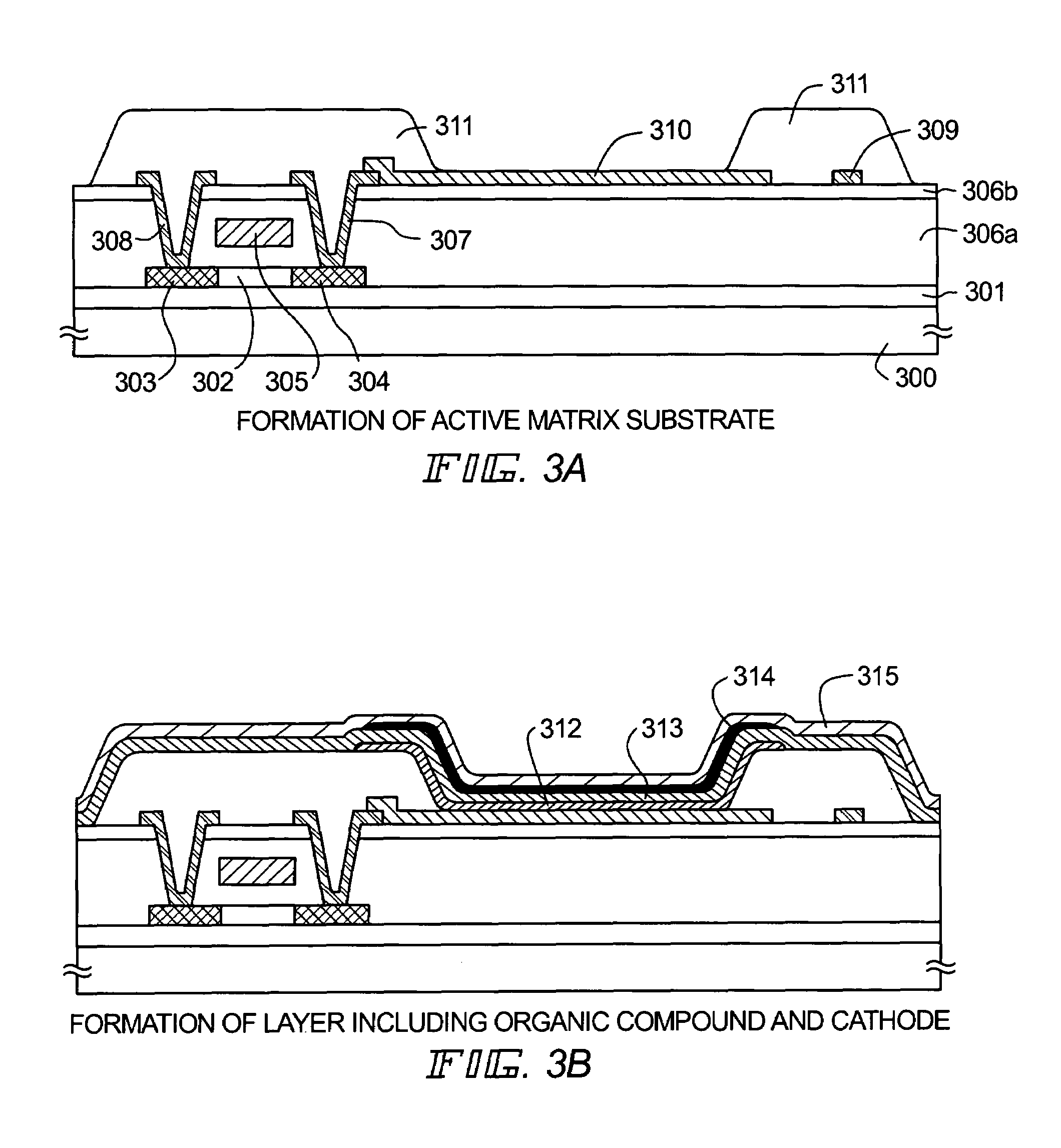
[0033]As shown in FIG. 3(A), a base film 301 is formed on a substrate 300 including an insulating surface. Next, a TFT is formed. An anode (pixel electrode) 310 connected to a drain electrode or a source electrode 308 and 307 of the TFT is formed. A metal with a large work function (Pt, Cr, W, Ni, Zn, Sn, In) is used as the anode. In the present embodiment, a conductive film comprising ITO formed by sputtering is used. The TFT comprises a gate electrode 305, a channel forming region 302, a source region or a drain region 303 and 304, the drain electrode or the source electrode 308 and 307, and insulating films 306a and 306b. Here, a p-channel type TFT, which is a semiconductor film (representatively, a polysilicon film) where the channel forming region is a crystalline structure, is described as an example of the TFT.
[0034]The uppermost layer of the interlayer insulating film of the TFT, i.e., the insulating layer 306b contacting the lower surface of the anode 310 is an inorganic in...
embodiment
Embodiment 1
[0051]The configuration of an active matrix type light-emitting device in which a TFT is disposed on each pixel is described as an embodiment of the invention. FIG. 4(A) is a top view thereof and FIG. 4(B) is a cross-sectional view cut along chain line A–A′.
[0052]In FIG. 4(A), reference numeral 1 is a source signal line driving circuit, reference numeral 2 is a pixel portion and reference numeral 3 is a gate signal line driving circuit. Also, reference numeral 4 is a sealing substrate, reference numeral 5 is a sealant, and the inner area surrounded by the sealant 5 serves as a space filled with an inert gas dried by a desiccant (not shown). Reference numeral 7 is a connection region where an upper electrode shared by light-emitting elements is connected to wiring on the substrate.
[0053]Video signals and clock signals are received from an FPC (flexible printed circuit) 6 serving as an external input terminal. Here, only the FPC is shown, but a printed wiring board (PWB) m...
PUM
| Property | Measurement | Unit |
|---|---|---|
| thickness | aaaaa | aaaaa |
| thickness | aaaaa | aaaaa |
| melting point | aaaaa | aaaaa |
Abstract
Description
Claims
Application Information