Flexible charge trap storage based on oxidized graphene

A technology of charge trap and charge trap layer, which is applied in the direction of electric solid-state devices, circuits, electrical components, etc., can solve the problems of performance impact, unstable performance of organic materials, and vulnerability to environmental influences, so as to reduce thermal budget, pinholes, etc. Less, the effect of ensuring the performance of the device

Inactive Publication Date: 2014-01-01
FUDAN UNIV
View PDF2 Cites 11 Cited by
  • Summary
  • Abstract
  • Description
  • Claims
  • Application Information

AI Technical Summary

Problems solved by technology

Although all organic materials can solve some problems, the performance of organic materials is unstable and easily affected by the environment
The performance of the device is bound to be severely affected by the

Method used


Image

  • Flexible charge trap storage based on oxidized graphene
  • Flexible charge trap storage based on oxidized graphene
  • Flexible charge trap storage based on oxidized graphene

Examples


Embodiment Construction

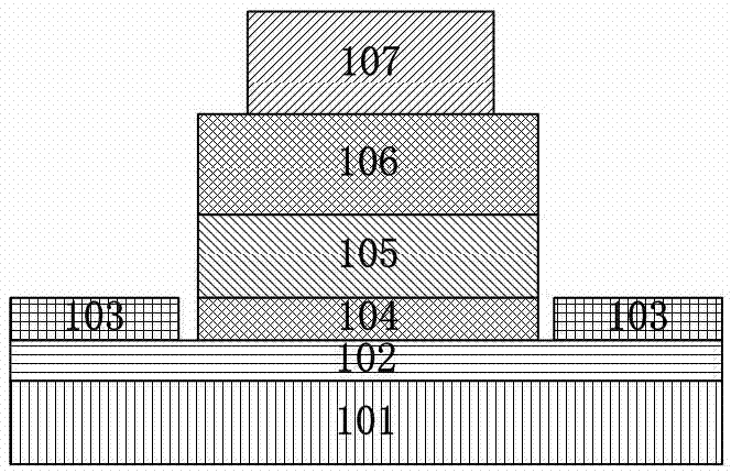
[0029] An exemplary embodiment of the present invention will be described in detail below with reference to the accompanying drawings. In the drawings, for convenience of description, the thicknesses of layers and regions are enlarged or reduced, and the shown sizes do not represent actual sizes. The representations in the referenced figures are schematic, but this should not be considered as limiting the scope of the invention. Also in the following description, the term substrate used may be understood to include the substrate being processed, possibly including other thin film layers prepared thereon.

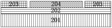
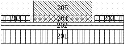
[0030] figure 1 A cross-sectional view of an example of a graphene oxide-based flexible charge trap memory provided by the present invention. Such as figure 2 As shown, the tunneling layer 104 formed by low temperature atomic layer deposition, the dielectric barrier layer 106 of the gate electrode, and the graphene oxide charge trap layer 105 are located on the flexible ...


PUM


Abstract

The invention belongs to the technical field of semiconductor devices and particularly relates to a flexible charge trap storage based on oxidized graphene and a preparation method thereof. According to the flexible charge trap storage and the preparation method, the storage relies on the three-layer structure of an existing charge trap storage, namely, the tunneling layer/charge trap layer/control gate dielectric layer structure, a flexible substrate is utilized as a substrate, and the oxidized graphene is adopted to replace the traditional charge trap layer. The method comprises the specific preparation steps of using a low-temperature atomic layer deposition method, firstly, depositing the dielectric tunneling layer on the flexible substrate, coating the flexible substrate with the oxidized graphene in a rotating mode under the indoor temperature situation, and then, similarly adopting the low-temperature atomic layer deposition technology to grow and control the gate dielectrics. The flexible charge trap storage and the preparation method have the advantages that the low-temperature atomic layer deposition technology and the process of coating the flexible substrate with the oxidized graphene at the indoor temperature in the rotating mode are used, the characteristics of the oxidized graphene is utilized, window erasing is ensured, meanwhile, the process thermal budget is greatly reduced, and practical and reliable schemes are provided for flexible electronic devices in future.

Description

technical field [0001] The invention belongs to the technical field of semiconductor devices, and in particular relates to a flexible charge trap memory. Background technique [0002] With the development of integrated circuits, people's demand for semiconductor devices is not limited to the increase in performance, but extends to more aspects. For example, flexible devices can be folded and curled. This feature makes it possible for applications in complex environments. [0003] One of the difficulties encountered in the development of flexible electronic devices is that flexible organic substrates cannot withstand high temperatures, so the necessary thermal budget in the device manufacturing process must be reduced. So the tunneling layer, the charge trapping layer, and the blocking layer must be grown at an appropriate lower temperature. Although the use of all organic materials can solve some of the problems, the performance of organic materials is not stable and is e...

Claims


Application Information

Patent Timeline
Patent Type & Authority Applications(China)
IPC IPC(8): H01L27/115H01L29/51H01L29/792H01L29/12
Inventor 孙清清王鲁浩王鹏飞张卫周鹏
Owner FUDAN UNIV
Why Eureka
Try Eureka