Organic transistor and method for producing the same

Inactive Publication Date: 2010-09-23
SHARP KK
View PDF2 Cites 11 Cited by
  • Summary
  • Abstract
  • Description
  • Claims
  • Application Information

AI Technical Summary

Benefits of technology

[0030]According to the structure of the organic transistor of the present invention and the method for producing the same, the second covalent bond and another second covalent bond adjacent to each other form a hydrogen bond in the direction of the plane perpendicular to the stacking direction of the stacked molecular film, that is, a direction approximately parallel to the surface of the gate electrode, thereby allowing production of a gate insulating layer under a mild condition, in which the interaction between neighboring molecules is strengthened and pinholes are unlikely to form.
[0031]In addition, by stacking two or more layers consisting of second organic molecular layers, the area of the hydrogen bond formed between the second covalent bonds adjacent to each other is increased in the stacking direction of the stacked molecular film, allowing further reduction of pinholes.
[0032]In addition, when the first organic molecular layer is composed of an aromatic ring, that is, a benzene backbone, it is possible to stack a molecular layer having a molecular structure that is upright in a substantially vertical direction with respect to the gate electrode.
[0033]In addition, when the second organic molecular layer is composed of a backbone having alkane as a main chain, the mobility of electrons is lowered by a sigma bond of the main alkyl chain and the insulating property of the molecular layer itself is improved to the stacking direction of the molecular layer.
[0034]In addition, when the end group at a side opposite to the gate electrode of the stacked molecular film is a phenyl group or a methyl group, arrangement of the organic molecules of the surface of the gate insulating layer, that is, the organic semiconductor layer contacting with the end group at the side opposite to the gate electrode of the stacked molecular film is improved by the hydrophobic surface of the phenyl group or the methyl group, allowing enhancement of the carrier mobility of the organic semiconductor layer.
[0035]In addition, when the first covalent bond is a siloxane bond, the first organic molecular layer is composed of a benzene backbone, the second covalent bond is an amide bond, and the second organic molecular layer has a backbone having alkane as the main chain, it is possible to obtain an insulating layer in which the molecular density in the stacked film is higher and flatness of an upper surface of the gate insulating film formed is higher.

Problems solved by technology

However, inorganic oxides such as a silicone oxide film or polymer materials such as polyimide (film thickness: approximately 100 nm to 300 nm) are generally used for their gate insulating layers, and the driving voltage is as high as 20 V to 100 V. With such a high driving voltage, damage to the organic compound and increase of electric power consumption are concerned, and therefore actual use is difficult.
Therefore, production at a low temperature and without the use of a vacuum process is difficult.

Method used


Image

  • Organic transistor and method for producing the same
  • Organic transistor and method for producing the same
  • Organic transistor and method for producing the same

Examples


example 1

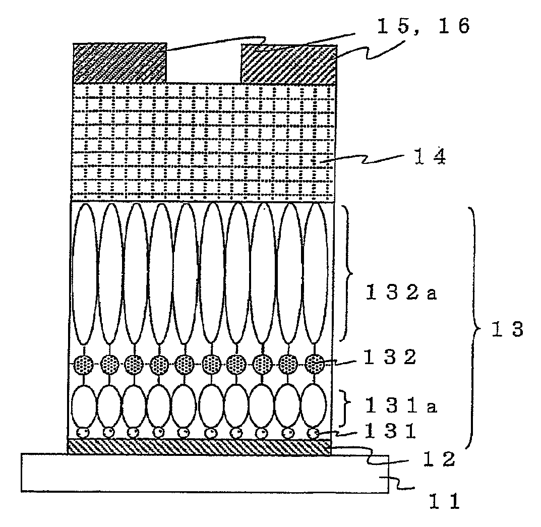
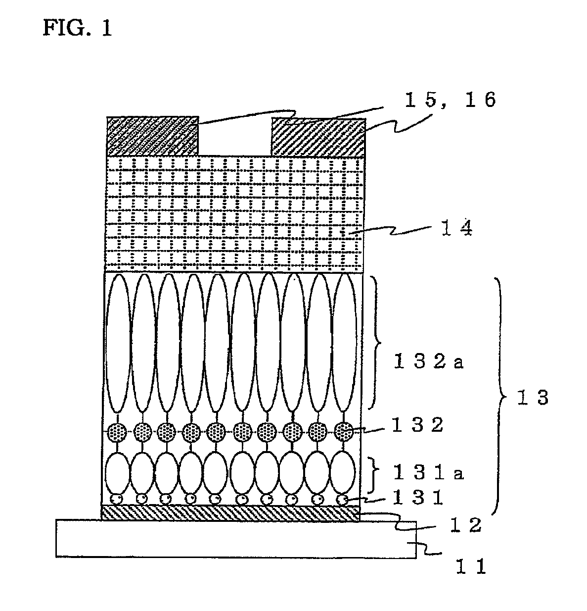
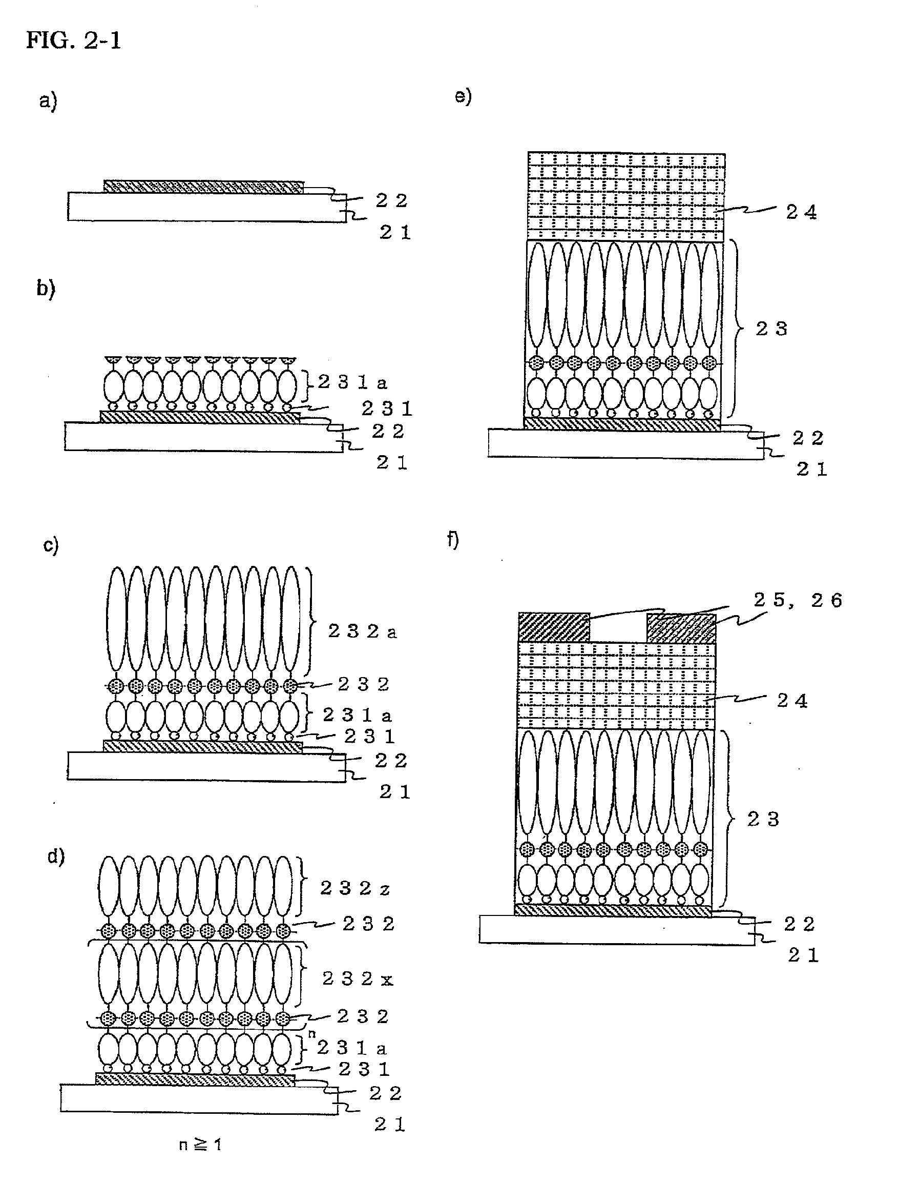
[0190]FIGS. 3a) to 3e) are drawings schematically illustrating a method for producing an organic transistor of the present invention.

[0191]First, 60 nm of aluminum was formed on a glass substrate 31 as a gate electrode 32 by vacuum deposition as illustrated in FIG. 3a). Next, the thus obtained was immersed in acetone to be delipidated by ultrasonic cleaning, and then a natural oxide film was formed on a surface of the aluminium formed into a film by oxygen plasma treatment, thereby exposing hydroxy groups on the surface.

[0192]Next, a first organic molecular layer 331a was formed through a first covalent bond 331 as illustrated in FIG. 3b). The substrate on which the electrode was formed and p-aminophenyltrimethoxysilane as an organic molecule for forming the first organic molecular layer were enclosed into a Teflon (registered trademark) vessel under a nitrogen atmosphere and heated in an oven at 100° C. for 120 minutes to form a first organic molecular layer having a phenyl backbon...

example 2

[0199]A gate electrode 42 and a first organic molecular layer 431a were formed on a glass substrate 41 as illustrated in FIGS. 4a) and b) in the same manner and using the same materials as in Example 1.

[0200]Next, a second organic molecular layer 432a was stacked on the first organic molecular layer 431a through a second covalent bond 432 as illustrated in FIG. 4c). Specifically, the substrate on which the first organic molecular layer was formed was immersed in 1 mmol / L of a methylene chloride solution of 6-phenylhexanoic acid as an organic molecule for forming the second organic molecular layer, and EDC was added thereto so that the concentration of the EDC would be 1 mmol / L and stirred at room temperature for 6 hours. Lastly, ultrasonic cleaning was carried out with chloroform to remove the 6-phenylhexanoic acid physically adsorbed on the substrate, thereby stacking an alkyl main chain formed through an amide bond and the second organic molecular layer having a phenyl group at an...

example 3

[0205]A first organic molecular layer 531a was formed on a gate electrode 52 on a glass substrate 51 through a first covalent bond 531 as illustrated in FIGS. 5a) and b) in the same manner and using the same materials as in Example 1.

[0206]Next, a second organic molecular layer 532a was stacked on the first organic molecular layer 531a through a second covalent bond 532 as illustrated in FIG. 5c). Specifically, the substrate on which the first organic molecular layer was formed was immersed in 1 mmol / L of an aqueous solution of glutaric acid, which is a bifunctional carboxylic acid as an organic molecule for forming the second organic molecular layer, and EDC was added thereto so that the concentration of the EDC would be 1 mmol / L and stirred at room temperature for 1 hour.

[0207]Next, a second organic molecular layer 532b was stacked on the second organic molecular layer 532a through the second covalent bond 532 as illustrated in FIG. 5d). Specifically, the substrate on which the se...


PUM


Abstract

An organic transistor comprising:at least a gate electrode and a gate insulating layer formed on the gate electrode,the gate insulating layer including, on a surface of the gate electrode, a stacked molecular film composed ofa first organic molecular layer binding in a direction substantially perpendicular to the surface of the gate electrode through a first covalent bond anda second organic molecular layer binding to an unreacted end of the first organic molecular layer through a second covalent bond, whereinthe second covalent bond and another second covalent bond adjacent to each other form a hydrogen bond in a direction of a surface perpendicular to a major axis direction of the stacked molecule.

Description

TECHNICAL FIELD[0001]The present invention relates to a field effect transistor (hereinafter, referred to as organic transistor) using an organic compound. More particularly, the present invention relates to an organic transistor that can be driven at a low voltage.BACKGROUND ART[0002]In recent years, organic transistors have attracted attention as a next-generation device to be an alternative to transistors of inorganic semiconductors such as silicon.[0003]As for the organic transistors, the devices can be produced at a lower temperature of 200° C. or less compared with the silicon semiconductor production process. Also, the organic transistor devices can be produced in a liquid-phase process that does not need a vacuum such as a printing method including inkjet and a spin coat method by dissolving an organic compound. Therefore, the devices can be produced on a plastic substrate and are expected to be applied to flexible devices such as electronic papers and electronic tags. Furth...

Claims


Application Information

Patent Timeline
IPC IPC(8): H01L51/30H01L51/10H01L51/40
CPCH01L51/052H01L51/0545H01L51/0533H10K10/471H10K10/476H10K10/466
Inventor KAMURA, MASAKAZUAOMORI, SHIGERUKUZUMOTO, YASUTAKA
Owner SHARP KK
Why Eureka
Try Eureka